Facebook
 Google
 GitHub
 Linkedin
Polycrystalline-SiC-Based Substrate Boosts Performance of SiC Power Devices
Learn how SmartSiC technology using Smart Cut overcomes standard Silicon Carbide limitations, reducing CO2 emissions, boosting device efficiency and reliability, and enabling more compact power modules.
This article is published by EEPower as part of an exclusive digital content partnership with Bodo’s Power Systems.
The rapid expansion of the electric vehicle market in recent years has placed immense pressure on the supply chain for high-quality Silicon Carbide (SiC) substrates. Standard substrate manufacturing methods are inefficient. Indeed, while standard SiC power devices are essential for "green" technologies, producing them is highly energy-intensive.

Image used courtesy of Adobe Stock
More often than not, power applications require devices that can handle higher currents with minimal energy loss to improve overall system efficiency and reduce cooling requirements. In hard switching conduction, power losses caused by the body diode‘s reverse recovery charges significantly erode efficiency at operating temperatures, well above 100°C in many cases. Standard methods to reduce these charges typically result in an unwanted increase in the forward voltage drop, thus increasing conduction losses.
Additionally, automotive and industrial applications require extreme reliability under harsh operating conditions. Standard SiC devices face specific failure mechanisms, such as Bipolar Degradation and thermal stress from Power Cycling at the power module level.
To address these bottlenecks, the manufacturing process of SmartSiC substrates, which employs Smart Cut™ technology, significantly decreases the CO2 emissions, allowing more sustainable manufacturing. During the use phase, this engineered substrate boosts efficiency through a reduction in on-resistance and a substantial decrease in reverse recovery energy without compromising the body diode‘s forward voltage. Furthermore, it enhances reliability through a demonstrated extended power cycling lifetime and provides robust immunity against bipolar degradation drift.
Technology Overview
Smart Cut is a semiconductor material layer transfer technology used to manufacture engineered substrates. The SmartSiC technology uses the Smart Cut process and involves a sequence of steps that allow a thin layer of a high-quality single-crystal SiC (monoSiC) wafer to be transferred onto a polycrystal SiC (polySiC) wafer (Figure 1).
Note: SmartSiC™ and Smart Cut™ are registered trademarks of Soitec S.A. Subsequent mentions in this text omit the trademark symbol for readability, but they are understood to carry this designation.
The process begins with the implantation phase, where a high-quality monoSiC wafer (called "donor") undergoes hydrogen ion implantation through its carbon face. This creates a weakened layer or "splitting plane" at a precise depth beneath the surface. The donor wafer is then bonded on the same face to a "handle" wafer made of polySiC with ultra-low electrical resistivity (2 mΩ·cm typ.) and enhanced mechanical properties. Then, layer detaching occurs along the plane weakened by the hydrogen implantation. This leaves a thin and high-quality monoSiC layer (typically below 1 µm thickness) transferred onto the polySiC handle. The resulting composite wafer is annealed at high temperature, making the bonding interface between monoSiC and the underneath polySiC highly electrically and thermally conductive. Finally, the surface of the transferred layer is polished to make it ready for epitaxial growth (epi-ready) [1] [2] [3].
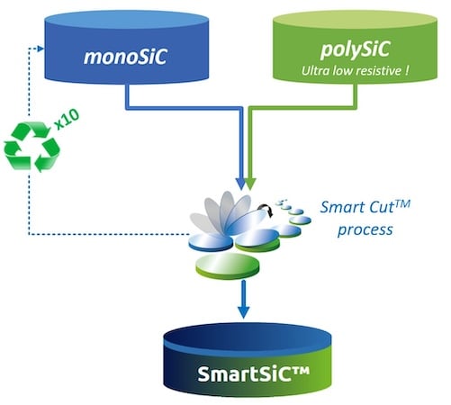
Figure 1. SmartSiC engineered substrate process overview. Image used courtesy of Bodo’s Power Systems [PDF]
From Substrate Features to Power Device Performance
The SmartSiC substrate value proposition is built on three main pillars - Performance, Reliability, and Sustainability - offering a greener, safer, and better performance at the system level, as illustrated in Figure 2.
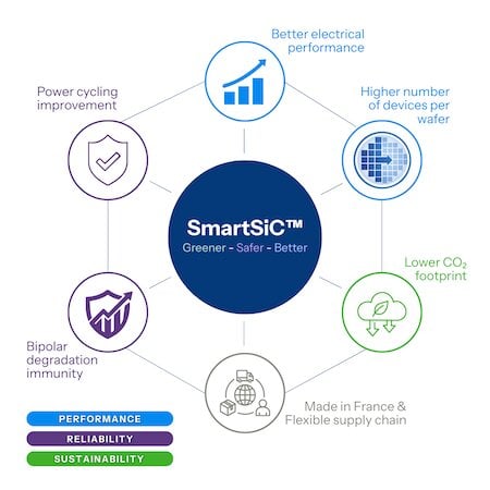
Figure 2. SmartSiC value proposition. Image used courtesy of Bodo’s Power Systems [PDF]
The SmartSiC technology minimizes the investment (CAPEX) in SiC boule manufacturing by drastically improving raw material utilization. This efficiency gain is a core part of its sustainability value proposition.
SmartSiC substrates significantly improve the electrical performance of SiC power devices (diodes and transistors) while maintaining compatibility with both 150mm and 200mm production lines, as well as with future SiC 300mm production lines.
The more immediate gain offered by SmartSiC substrates is to leverage the overall current density of the power devices. This makes it possible, for a given device on-resistance, to increase the number of devices per wafer, or to reduce the number of devices per module, at a given device size.
Moreover, the high doping level of the polySiC handle wafer allows for the formation of backside ohmic contacts via tunneling current without the need for the laser annealing required for standard monoSiC substrates. Skipping this process step will have a non-negligible impact on the OPEX and CAPEX, as well as on overall manufacturing yield.
The hydrogen implantation step, intrinsic to the Smart Cut process, enhances the dynamic performance of the final devices, and it contributes to improving the mechanical and reliability characteristics of the device.
Reducing Conduction Losses
SmartSiC utilizes a polySiC handle wafer with ultra-low resistivity, typically 2 mΩ·cm, compared to 20 mΩ·cm for standard monoSiC [1] [2] [3].
This low resistive substrate, combined with the capability to form lower resistivity metal contacts on the backside of the power devices, leads to a significant reduction in the specific on-resistance of the device, depending on the voltage class and generation [1] [3].
As an example, the results in Figure 3 demonstrated that 13 mΩ 650 V Gen2 planar SiC MOSFETs (from STMicroelectronics), manufactured on SmartSiC substrates, achieve an average RDSon reduction of approximately 24% compared to those built on standard monoSiC wafers [1].
This performance enhancement is significant enough to be comparable to the gains typically realized when transitioning from one device generation to the next one.
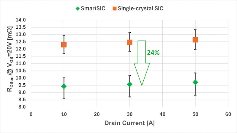
Figure 3. RDSon comparison for SiC MOSFET manufactured with monoSiC and SmartSiC substrates [1]. Image used courtesy of Bodo’s Power Systems [PDF]
In parallel, 1200V MOSFETs with an initial specific resistance of 2.8 mΩ·cm² exhibit an RDSon reduction of 15%, while future generations are projected to see reductions exceeding 20% [1].
The most immediate consequence of low RDSon is the minimization of conduction losses. In power MOSFETs, the specific on-resistance is a primary contributor to energy loss during the "on" state. The reduction in conduction losses is critical for achieving high-efficiency targets, such as the 80 Plus Titanium or Ruby standards for power supply units (PSU) in future AI data centers. It also reduces the thermal stress on the system, potentially allowing for smaller heatsinks and fans
Low RDSon enables a more efficient use of the semiconductor surface area. Devices with lower specific resistance (RDSon.A) can handle higher current density. This characteristic allows manufacturers to reduce the device die size (chip shrinking) while maintaining the same current rating as a larger, standard device. This is particularly advantageous for power devices, increasing the productivity per wafer and facilitating more compact package designs.
Moreover, a lower resistive substrate contributes to a reduced voltage drop in diodes, whether in unipolar Schottky (VF) or during third-quadrant conduction (VSD) of MOSFETs (body diode conduction). For MOSFETs, particularly during dead-time in hard switching conditions, the operation of the device in the third-quadrant is inevitable.
Reducing Switching Power Losses
The optimization of reverse recovery characteristics ensures that total switching losses are minimized, thereby maximizing converter efficiency.
Power devices built on SmartSiC substrates exhibit a significant reduction in reverse recovery charges (Qrr). This is attributed to a reduced carrier lifetime and lower hole density near the buffer interface.
Indeed, the hydrogen implantation of the Smart Cut technology creates recombination centers near the bonding interface. These centers reduce the minority carrier lifetime, resulting in a 33% to 41% reduction of Qrr at high temperatures: see figure 4 [4] [5] [6].
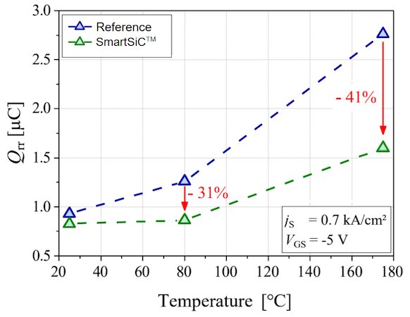
Figure 4. Body diode Qrr comparison for a 12 mOhm / 1200 V Gen1 SiC MOSFET manufactured in single-crystal SiC and SmartSiC substrates [4]. Image used courtesy of Bodo’s Power Systems [PDF]
What is more, SmartSiC achieves this without degrading the body diode‘s forward voltage drop, thereby breaking the traditional trade-off between switching speed and conduction loss.
Bipolar Degradation Immunity
An added advantage of the SmartSiC substrates is their inherent immunity to bipolar degradation. The hydrogen implantation has been evidenced to minimize the occurrence of Shockley Stacking Faults (SSFs) [7]. This makes the substrates highly robust against bipolar degradation, a common failure mode where RDSon increases over time.
Figure 5 shows a significant forward voltage drift under high-current stress (600sec-2250 A/cm2) of a 1200V-10A PiN diode made on a standard 4H-SiC wafer. The same electrical results for a 1200V-10A SmartSiC-based PiN diode have shown no visible voltage drift after the same stress test [2].
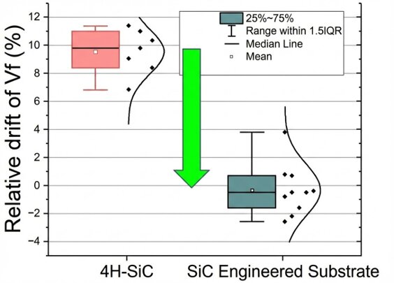
Figure 5. Pre & Post stress forward voltage drop comparison of 4H-SiC & SmartSiC 1200V-10A PiN diode [2]. Figure 6: Comparison of standard SiC and SmartSiC substrates lifetime assembly for both silver sintering [3]. Image used courtesy of Bodo’s Power Systems [PDF]
Increasing Device Lifespan With Higher Power Cycling Capability
This power cycling lifetime improvement primarily occurs through the superior mechanical properties of the polySiC, which reduces the stress on the device‘s die attach.
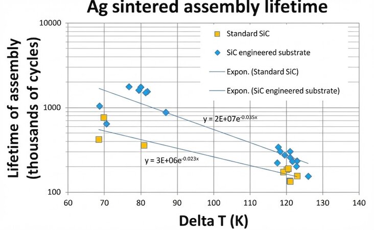
Figure 6. Comparison of standard SiC and SmartSiC substrates lifetime assembly for both silver sintering [3]. Figure 6: Comparison of standard SiC and SmartSiC substrates lifetime assembly for both silver sintering [3]. Image used courtesy of Bodo’s Power Systems [PDF]
The polySiC handle possesses a lower Young‘s modulus compared to standard monoSiC (approximately 93% of the value). This results in a semiconductor die that is less stiff, hence lowering the plastic strain per cycle exerted on the packaging layers during thermal expansion and contraction, providing extended power cycling lifetime when compared to standard SiC substrates [3] [8].
Experimental results showed that SmartSiC substrates enable a potential increase in maximum junction temperature of around 20K higher than standard SiC wafers, without compromising the reliability (see figure 6).
Enabling a Greener Manufacturing Process
Smart Cut technology significantly enhances Silicon Carbide manufacturing by enabling the reuse of donor wafers, increasing the number of SiC wafers obtainable from a single SiC boule by a factor of 10-fold.
This process replaces resource-intensive, week-long growth cycles at temperatures exceeding 2000°C with more efficient chemical vapor deposition methods that operate below 1500°C during a couple of days.
By combining this superior material efficiency with a drastically reduced energy profile, the SmartSiC approach achieves a 75% reduction in total carbon dioxide emissions compared to traditional SiC wafer production methods.
Conclusion
SmartSiC technology overcomes the scalability and efficiency limitations of standard Silicon Carbide. It offers a combination of significant reduction in manufacturing carbon footprint and power electronics performance improvement while providing superior reliability for the end applications. This leverages the design of compact power modules that are foreseen for the next generation of space-constrained Electrical Vehicle, Photovoltaic, and AI data center power supplies. Additionally, for high voltage applications such as Rail traction or Renewable energy grids, the SmartSiC crystal quality and immunity to bipolar degradation ensure long-term reliability.
Note: SmartSiC™ and Smart Cut™ are registered trademarks of Soitec S.A. Subsequent mentions in this text omit the trademark symbol for readability, but they are understood to carry this designation.
References
[1] G. Picun et al., Engineered Substrates with ultra-low resistivity Polycrystalline SiC Base, Bodo’s Power, June 2024
[2] E. Guiot et al., SmartSiC 150 & 200mm engineered substrate: solving SiC power devices bipolar degradation, CS Mantech 2025
[3] E. Guiot et al., SmartSiC 150 & 200mm Engineered Substrate: Enabling SiC Power Devices with Improved Performances and Reliability, ICSCRM 2024
[4] M. Alaluss et al., Dynamic Characterization and Robustness of SiC MOSFETs Based on SmartSiC Engineered Substrates, ICSCRM 2024
[5] E. Guiot, Improvement of SiC MOSFETs body diode Qrr up to 30% through semiconductor substrate engineering, APEC 2026
[6] M. Alaluss et al., Plasma Behavior of SiC MOSFETs with Engineered Substrates during Reverse Recovery, ISPSD 2025
[7] Harada et al., Suppression of stacking fault expansion in a 4HSiC epitaxial layer by proton irradiation, Nature, Scientific Reports volume 12, Article number 13542 (2022)
[8] P. Heimler et al., Impact of different SiC substrate technologies on the Power Cycling Capability of SiC-MOSFETs, CIPS 2026
This article originally appeared in Bodo’s Power Systems [PDF] magazine.