Facebook
 Google
 GitHub
 Linkedin
Enhanced Trench IGBTs and Field Charge Controlled Diode: The Next Leap in IGBT and Diode Performance
This article discusses the future generation of IGBT modules which will employ Enhanced Trench ET-IGBTs and Field Charge Extraction and their benefits.
Future generations of IGBT modules will employ Enhanced Trench ET-IGBTs and Field Charge Extraction FCE diodes capable of providing higher level of electrical performance in terms of low losses, good controllability, high robustness and soft diode reverse recovery.
Despite the fact that the Insulated Gate Bipolar Transistor (IGBT) and antiparallel diode have experienced over the past two decades important breakthroughs with respect to the device process and design concepts which resulted in clear leaps in device overall performance, further development work is underway to achieve the next level in terms of higher power densities, improved controllability and robustness. In this article, we will first briefly discuss the current IGBT and diode development trends while focusing on the next-generation technologies; namely the Enhanced Trench IGBT (ET-IGBT) and Field Charge Extraction (FCE) diode. Then, the new device concepts and their electrical performance will be demonstrated for the 3.3 kV voltage class.
IGBT and diode future development trends
The main three IGBT development trends today are targeting higher power densities with (a) Enhanced Trench ET-IGBTs, (b) higher operating temperatures above the traditional 125°C mark and (c) IGBT/ Diode integration solutions referred to as Reverse Conducting RCIGBT or Bi-mode Insulated Gate Transistor (BIGT). In the BIGT case, the single-chip approach provides improved performance especially with respect to the limitations due to the restriction in available diode area depending on the given application requirements. Nevertheless, the traditional IGBT/Diode two-chip approach remains as an important development path for many mainstream applications. Today, state-of-the-art high voltage devices with a similar loss performance employ Enhanced Planar IGBT (EP-IGBT) or Trench IGBT MOS cell concepts on Soft Punch Through (SPT) structures. However, for lower voltage devices rated below 2 kV, in addition to trench IGBTs, advanced ET-IGBTs are already an established technology. Furthermore, the ET-IGBT concept is also capable of providing the next step in loss reduction for high voltage IGBTs. Figure 1 demonstrates the on-state Vce(sat) loss reduction of a 3300 V IGBT for the same turn-off losses Eoff achieved with the new ET-IGBT MOS cell on the same bulk SPT platform. However, it is important to point out that the trench based IGBTs, especially for higher voltage ratings, exhibit an inherently high effective gate input capacitance when compared to planar based devices which results in less controllability for optimum switching performance during IGBT turn-on. Overcoming this negative aspect combined with the lower losses of the ET-IGBT will provide an ideal solution for the next generation high voltage IGBTs.
For the fast diode part, the losses and reverse recovery softness remain as a critical performance target for matching the performance of the new ET-IGBTs. The Field Charge Extraction (FCE) concept demonstrated that soft recovery performance under extreme switching conditions combined with low losses could be achieved while having no drawbacks on other electrical parameters.
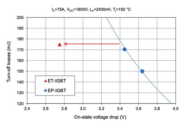
Figure 1: 3.3kV IGBT trade-off curve between on-state voltage drop and turn-off losses. Comparison between the enhanced trench (ET) and enhanced planar (EP) structures
The ET-IGBT concept
The main approach followed for the realization of the ET-IGBT concept with the targeted enhanced carrier concentration near the trench emitter for lower losses is based on the introduction of a striped active Trench MOS Cell with an n-enhancement layer. In order to reduce the effective input capacitance for improved switching controllability, the focus is on the optimization of the regions between the active cells, which contribute strongly to the device effective input capacitance value during switching. By eliminating gate regions between the active cells as shown in the cross-section in figure 2, we allow for a low effective gate emitter input capacitance compared to state-of-the-art trench IGBT designs while providing optimum reverse blocking capability. The lower on-state losses of the 3.3 kV ET-IGBT provides potentially a 20% increase in the rated current capability compared to the EP-IGBT generation.
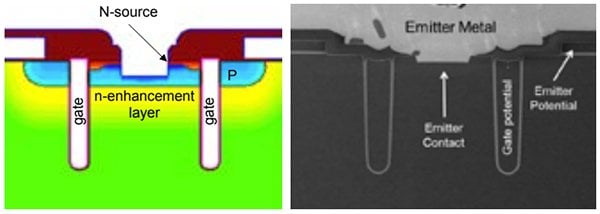
Figure 2: ET-IGBT MOS Cell concept
The FCE diode concept
For the new diode, a combination of the Field Charge Extraction (FCE) concept and the well-established Field Shielded Anode (FSA) design is utilized as shown in figure 3 when compared to a conventional design. The thickness of the n-base plays a key role for the overall loss generation where low-loss diodes require a thin n-base design. However, further reductions of the thickness of the n-base region have been typically restricted by the snappy reverse recovery behavior of the resulting diodes. By introducing small p-doped areas at the cathode side of the diodes as shown in figure 3, a field-induced carrier injection process is enabled during the recovery phase, which generates inherently soft diodes. Therefore, the n-base of a 3.3 kV rated diode can be thinned by 10% while the blocking capability is maintained by increasing the resistivity without compromising soft reverse recovery. The benefit of this approach is a 20% improvement on the technology curve. Moreover, the robustness of these inherently soft diodes has been improved due to the absence of large overshoot voltages during reverse recovery.
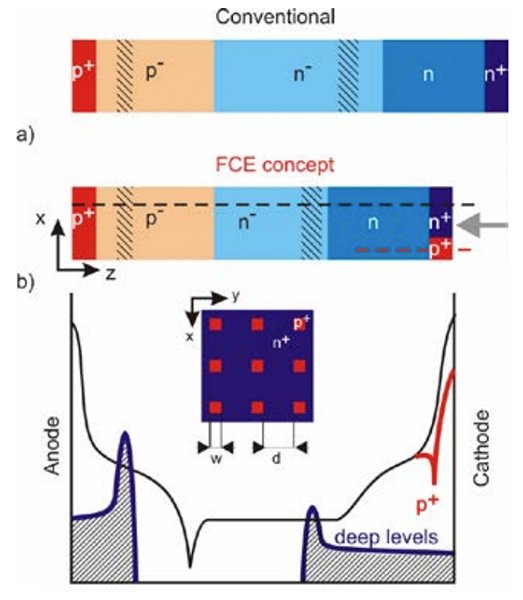
Figure 3: The combination of FCE and FSA concepts (a) and (b) cross sections, (c) doping profile
3.3 kV ET-IGBT module prototypes
3.3 kV ET-IGBT and FCE-diode chips were manufactured with an active area of approximately 1 cm2 per chip with a defined rating of 75 A for the IGBT and 150 A for the diode. The chips were employed in a standard high voltage insulated module (140 x 70) mm2 having a dual configuration as shown in the inset of figure 4. Each IGBT/diode part in the dual package consists of a single substrate containing 4 x ETIGBTs and 2 x FCE-diodes. The resulting current rating of the module is 300 A compared to today’s 250 A for an equivalent EP-IGBT.
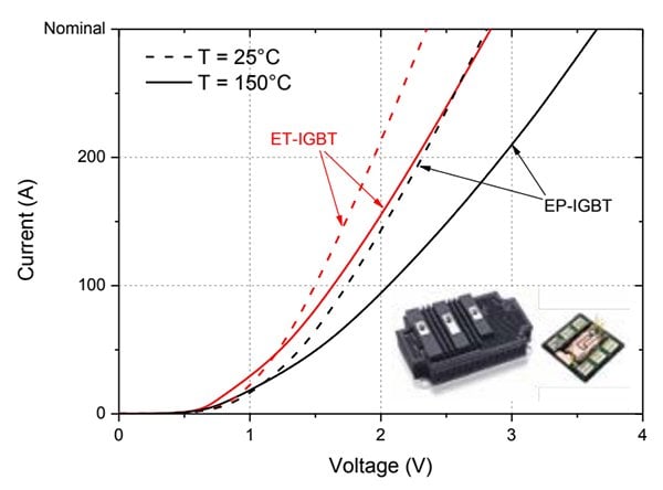
Figure 4: 300A/3.3kV ET-IGBT module output I-V characteristics at 25°C and 150°C.
The modules were tested electrically under static and dynamic conditions. Figure 4 shows the on-state characteristics for the ET-IGBT at 25°C and 150°C and compared to the EP-IGBT. The ET-IGBT module exhibits much lower static losses compared to the EP-IGBT together with strong positive temperature coefficient for safe paralleling of chips. At the rated current of 300 A, the ET-IGBT design has a Vce(sat) of 2.75 V compared to 3.55 V for the EP-IGBT at 150°C.
Figure 5 shows the nominal turn-off and turn-on switching waveforms for both ET-IGBT and the reference EP-IGBT, respectively. The test conditions were kept the same to better evaluate the device performance. The devices were switched against an applied DC-link voltage of 1800 V and a rated current of 300 A at 150°C with a gate emitter capacitance of 47 nF. The stray inductance was 600nH and the turnoff gate resistance was 9Ω while the turn-on gate resistance varied per design as indicated. The turn-off losses Eoff of the ET-IGBT were at around 650mJ compared to 600 mJ for the EP-IGBT. However, larger variations were obtained for the turn-on losses Eon where the ET-IGBT was at 860mJ albeit with a different gate resistor compared to 910 mJ for the EP-IGBT. The total switching losses for all tested devices were approximately at the same level just below 1.5 J. The FCE-diode reverse recovery performance can also be seen in the IGBT turn-on waveforms. The controllability of the ET-IGBT is illustrated in figure 6 when plotting the turn-on parameters (Icmax, Eon and di/dt) against the variation in the gate resistance.
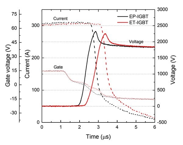
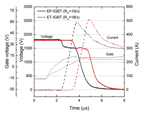
Figure 5: 300A/3.3kV module Turn-off (left) and Turn-on (right) waveforms (1800V, 300A, 150°C).
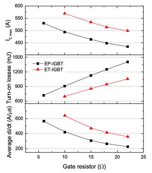
Figure 6: Effect of varying the gate resistance on the turn-on parameters (1800V, 300A, 150°C)
The FCE diode softness was also tested under the same circuit setup but at the critical softness conditions with a lower current of 15 A and a lower temperature of 25°C as shown in figure 7. The FCE diode clearly shows very soft recovery performance under these extreme conditions when compared to the standard diodes exhibiting a typical current snap-off along with the associated high overshoot voltage.

Figure 7: 300A/3.3kV module reverse recovery (1800V, 15A, 25°C).
ET-IGBT Turn-off and Short Circuit SOA Performance
The turn-off (RBSOA) behavior was tested for two paralleled chips under high current and voltage conditions. For the RBSOA, the ETIGBT was tested against a high DC-link voltage of 2500 V and the maximum achieved switchable current is approximately 5x and 4x the nominal current at 25°C and 125°C, respectively as shown in figure 8. The device enters and withstands both stress conditions known as dynamic avalanche and Switching Self Clamping Mode SSCM at 25°C. At a temperature of 125°C, the device experiences stronger dynamic avalanche as expected due to the higher levels of carrier concentrations which results in a lower but still sufficient turn-off capability.
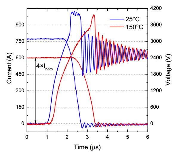
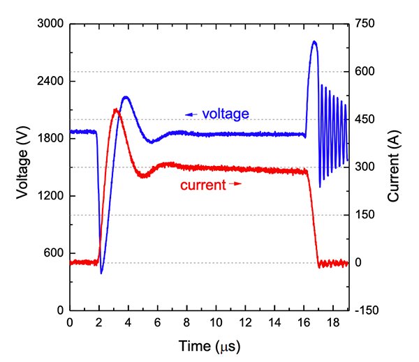
Figure 8: 3300V ET-IGBT Turn-off RBSOA (2500V, Rg=33Ω, Ls=2400nH, Vge=20V) and short circuit SOA (1800V, tsc=15us, Vge=15V, Rg=33Ω, Ls=2400nH, T=25°C) waveforms
The single-chip ET-IGBT short circuit test was carried out at 1800 V and 25°C and the resulting waveforms are shown in figure 8. At a short circuit current level of around 300 A, a smooth and stable behavior was obtained for pulse widths of at least 15 us.
With the above SOA performance, it is encouraging that the improvements achieved for lowering the on-state losses of the ET-IGBT have not compromised the device robustness, which is strongly required especially when targeting higher power densities for the next generation HiPak and LinPak modules.
About ABB
ABB is a pioneering technology leader with a comprehensive offering for digital industries. With a history of innovation spanning more than 130 years, ABB is today a leader in digital industries with four customer-focused, globally leading businesses: Electrification, Industrial Automation, Motion, and Robotics & Discrete Automation, supported by its common ABB Ability™ digital platform. ABB's market-leading Power Grids business will be divested to Hitachi in 2020. ABB operates in more than 100 countries with about 147,000 employees.
This article originally appeared in the Bodo’s Power Systems magazine.