Facebook
 Google
 GitHub
 Linkedin
An Exploration of Surface Mount Power Packaging Technologies for SiC MOSFETs
Surface-mount packaging for SiC MOSFETs boosts power density, reduces parasitics, and improves thermal performance compared to legacy packages, aiding efficient, compact high-power designs.
This article is published by EEPower as part of an exclusive digital content partnership with Bodo’s Power Systems.
The adoption of Wide-Bandgap (WBG) devices is driven by innovation in device technology and packaging. New and ongoing challenges in device technology require manufacturers to continually enhance and upgrade their devices. Surface mount packages for Silicon Carbide (SiC) MOSFETs and diodes offer several advantages over through-hole packages. Today, this is primarily driven by the need for compact, efficient systems that run cool. A SiC device lends itself to these benefits with its higher efficiency and current density.
Benefits
Historically, the 3-terminal TO-247 package has been the workhorse in power converters, accommodating large die but falls short in leveraging the performance advantages of WBG technology. The 4-terminal TO-247, or TO-247-4L, introduced the Kelvin source for reduced loop inductance and improved gate drive signal quality. However, it offered minimal improvements in thermal performance.
Within the surface mount family of discrete packages, designers may choose between top or bottom-side cooled packages. The selection criteria are driven by the following primary factors:
1. Power Density – Maximizes continuous and peak power capability from a given die while maintaining sufficient creepage and clearance distances
2. Electrical Performance – Minimizes parasitic inductance, reducing the overshoot and ringing as well as the overall switching losses
3. Ease of Use – Simplifies circuit board design while improving the design for manufacturability
4. Availability – Industry-standard packages offer the benefit of multi-sourcing while unique packages offer designers opportunities for differentiation
Table 1 summarizes JEDEC recognized surface mount packaging options that are generally available from multiple vendors.
Table 1. Package Characteristics
| Package | Approx. Dimensions (mm) | Approx. Creepage (mm) | Cooling | Notes |
| D2PAK | 15 x 10 x 4.3 | 6.6 | Bottomside | Heat conduction through circuit board |
| TOLL | 10 x 11 x 2.3 | 3.15 | Bottomside | |
| PSMT (TOLT) | 10 x 15 x 2.3 | 3.0 | Top-side | Low inductance, high power density |
| QDPAK | 15 x 21 x 2.3 | 4.8 | Top-side |
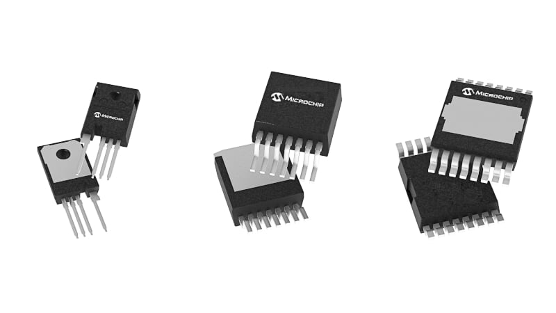
Figure 1. TO-247-4LN (left); D2PAK (center); PSMT (right). Image used courtesy of Bodo’s Power Systems [PDF]
Ease of Use
Balancing design considerations, such as thermal performance, assembly and reliability, is important when selecting a package. Topside cooled package feature options, such as positive and negative standoff, drive the circuit board layout design, thermal design, and assembly process. The standoff represents the z-axis offset from the bottom of the package body to the bottom of the leads.
With positive standoff, the leads sit flush on the printed circuit board (PCB), creating a gap between the package body and the board. This requires thicker Thermal Interface Material (TIM) to account for the gap and its tolerance and ensures proper compression for optimal thermal conductivity. However, excessive compression can stress solder joints, potentially leading to fatigue and reliability issues over time.
The negative standoff feature mitigates the reliability risk on solder joint fatigue by significantly reducing the stress on the device leads. With a negative standoff, the package body makes direct contact with the PCB substrate. A gap of 0.01–0.11 mm is maintained between the bottom of the package body and the bottom of the leads.
The thickness and thermal performance of the TIM depends on the package height and lead tolerance. A negative standoff minimizes the effect of lead tolerance, as solder fills the gap between the lead and the PCB pad. This allows the package body to consistently rest flat on the PCB, minimizing variations in TIM thickness due to tolerances. As a result, the junction-to-ambient thermal resistance is optimized and closely controlled, reducing solder joint stress and associated fatigue while improving long-term reliability.
Improving Power Density
This section presents simulation results comparing D2PAK and PSMT packages. The simulation aims to evaluate heat flux and cooling performance, using heat conduction through the PCB and TIM for bottom-side cooled D2PAK devices, and through the TIM and heatsink for top-side cooled PSMT devices.
A 100 µm thick TIM is applied between the PCB and the heat sink in the simulation with the D2PAK, and between the device and heatsink in the case of the PSMT simulation. Figure 2 below is a representation of the thermal conduction path.
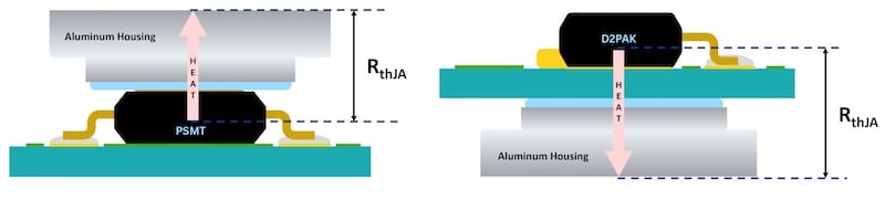
Figure 2. Thermal path in PSMT vs D2PAK. Image used courtesy of Bodo’s Power Systems [PDF]
Simulations were performed in free convection at 25°C and 85°C. Shown in Figure 3 are results from the 85°C simulation for the PSMT and D2PAK packages. The PSMT package simulation showed a 25% - 35% lower junction temperature than the D2PAK. A top-side cooled package offers a better thermal path, resulting in a lower junction temperature and higher power density system.
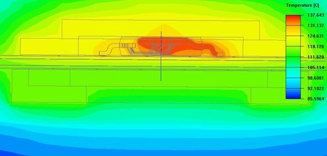
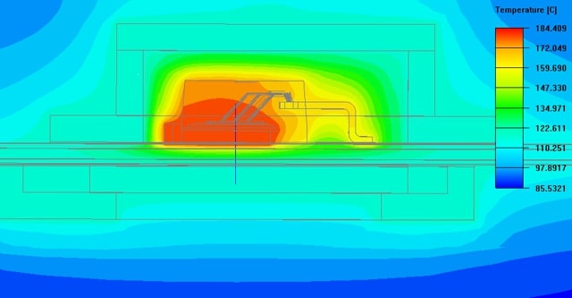
Figure 3. Thermal simulation results of PSMT (top) and D2PAK (bottom). Image used courtesy of Bodo’s Power Systems [PDF]
Impact of Creepage & Parasitic Inductance
Below are the simulation results for power loop inductance for different SiC power packages.
Table 2. Packages Simulation Results
| Package | Creepage | Inductance |
| TO-247-4LN | 8.45 mm | 31.97 nH |
| D2PAK | 6.6 mm | 29.89 nH |
| PSMT (TOLT) | 3.0 mm | 14.13 nH |
In designing high voltage systems, creepage distance is an important design parameter. The legacy TO-247 evolved from 3 lead (TO-247-3L) to 4 lead (TO-247-4L) to 4 lead with notch (TO-247- 4LN) increasing the creepage from 3.0 mm to 3.8 mm to 8.45 mm.
While important, there are design solutions for creepage, such as introducing a notch in the PCB or conformal coating. Table 2 provides a summary of the three packages. Parasitic inductance is a significant factor impacting power conversion efficiency. Parasitic inductance exists in both power and gate loops, influencing overall device performance. In high-frequency power converters utilizing SiC MOSFETs, parasitic inductance becomes increasingly problematic, resulting in greater energy losses, increased voltage overshoot and elevated Electromagnetic Interference (EMI) due to ringing. The impact of parasitic inductance can be visualized in the waveforms of Figure 4 by the voltage overshoot during switching.
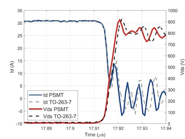
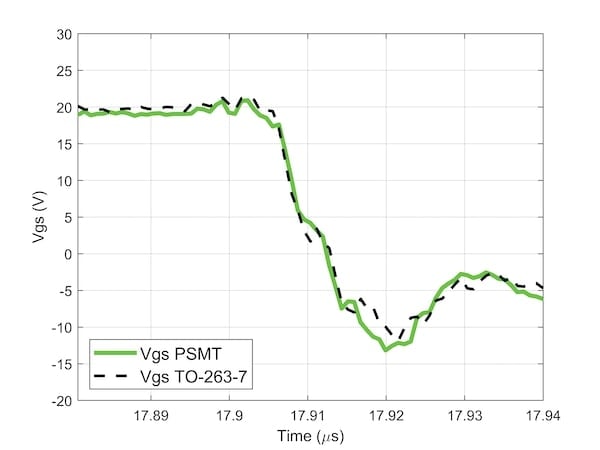
Figure 4. Switching waveforms comparing the D2PAK vs the PSMT. Image used courtesy of Bodo’s Power Systems [PDF]
Top-side cooled packages, such as PSMT and QDPAK, provide notable benefits compared to bottom-side cooled options, such as D2PAK and TOLL. By separating the thermal and electrical paths, these devices enable system designers to reduce parasitic inductance and optimize thermal management. This separation allows for more flexible and efficient power loop routing. With the electrical path independent from the thermal path, designers can better minimize inductive losses, support faster switching speeds in their applications and increase power density.
Summary
Top-sided cooled package offers excellent thermal improvements over legacy discrete packages. If the designer is trying to optimize switching or simplify their manufacturing, Microchip has a wide array of other packages offered in voltage ranges of 700V to 3300V.
Beyond discrete packaging, as power requirements increase, integration could be key to solving the power density or switching efficiency problems.
This article originally appeared in Bodo’s Power Systems [PDF] magazine.