Facebook
 Google
 GitHub
 Linkedin
Designing Electronics to Pass the EMC Test Part 4
Simulating and evaluating the conductive emission using LTSpice.
In Part 1, Part 2, and Part 3, we studied the Conductive Emission (CE) path and learned how to model the LISN and passive components. I have explained why getting the correct model for all the passive components, like capacitors and inductors, is essential.
We have also learned how to calculate the parasitic capacitor between our EUT and the EMC lab earth plates.
It's time to do some examples of how I evaluate the common mode (CM) and differential mode (DM) noise using LTSpice, and how you can assess the emissions of your circuits.
In Part 4, we will see:
- How to use LTSpice to simulate the CM and DM noise from a LISN,
- Using the wrong model for capacitors and inductors brings inaccurate results and where to download the LTSpice models.
- How to convert Voltage to dbuV in LTSpice and how to see the CM and DM noise.
- How to use the FFT from LTSpice to see the conductive emission up to 1 GHz.
- How to use a CM choke to reduce the CM emission.
Designing a 3.3 V Buck Converter
In most of my DC/DC converter designs, I predominately use the DC/DC converters from Analog devices. One of the main reasons is that, as we will learn here, we will save a lot of time on our design since AD lets us simulate their DC/DC converter with the excellent tool LTSpice.
Linear Technology originally designed LTSpice in 1999, and it has been my tool for analog simulations for more than 20+ years. It is compelling, and I don’t remember if I had a simulation that didn’t reflect what I have seen in the field.
Suppose we want to design a 10 V to 3.3 V buck converter, 1A. We can select one of many DC/DC converters from the AD website. I have chosen LT3971-3.3 since it requires only a few extra components. So let's open the LT3971-3.3 datasheet, copy the reference schematic, and run our first simulation with LTspice.
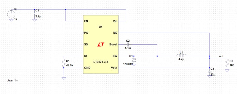
Figure 1. The LT3971-3.3 schematic as shown in the datasheet. (using ideal passive components). Image used courtesy of Francesco Poderico
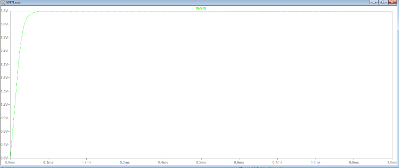
Figure 2. Running the first simulation. Image used courtesy of Francesco Poderico
The first thing to notice is that the DCDC converter requires less than 0.1 msec to stabilize the output. Let's take note of this (we will need it later).
Let's zoom the Vout now and see the typical saw waveform studied at university.
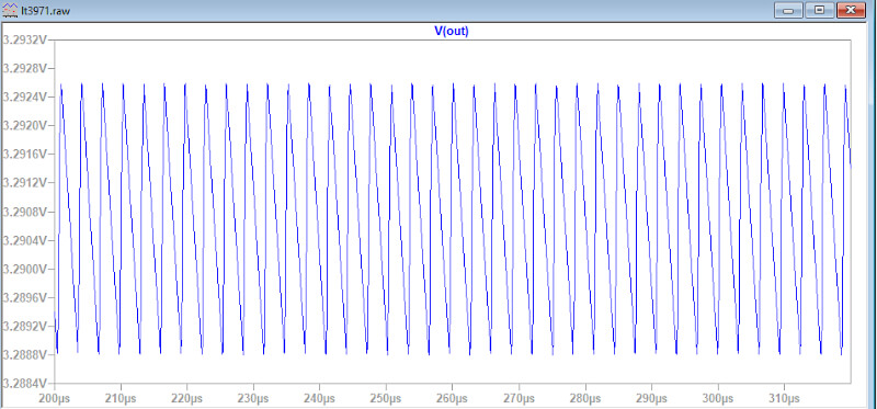
Figure 3. By zooming the Vout, we can see the typical saw wave waveform of an ideal buck converter. Image used courtesy of Francesco Poderico
All good! Or not?
The issue is that we are not using the correct models for the passive elements L1, C1, C2, and C3.
Let's repeat the same simulation using some models for L1, C1, C2, and C3. Let's repeat the simulation using the correct models for L1, C1, C2, and C3 and see what difference it makes.
For this article, we will use Wurth components. The nice thing about Wurth is that they have created a tremendous library for LTSpice, Altium, etc. So let's go on Wurth and download some LTspice library, which we need for this simulation.
I have downloaded the library:
LTSpice_WE-LQFS, LTSpice_WE-CNSW, LTSpice_WCAP_ASLU, LTSpice_WCAP_CSGP
They are available free of charge from the Wurth website. Please download and copy in C:\Users\yourname\Documents\LTSpiceXVII\lib.
Once we have done this, we can use this library for our project. Let's run the same simulation but use the correct model for all the passive.
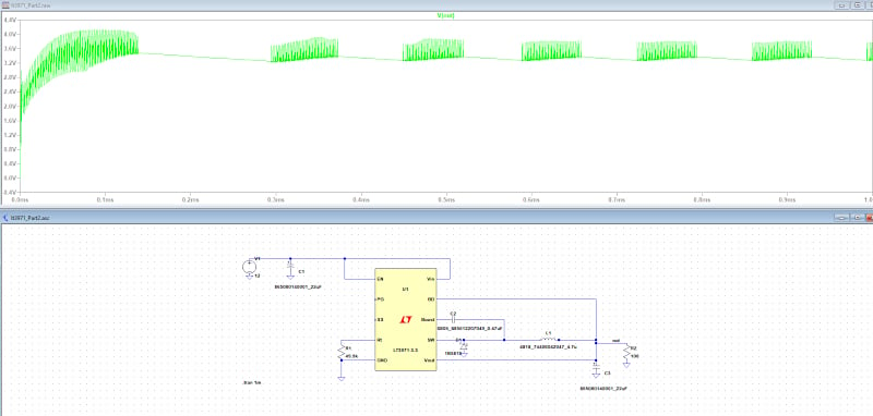
Figure 4. The simulation above is a perfect example that shows why we should use capacitors with Low ESR for a DCDC converter. Image used courtesy of Francesco Poderico
We have the first surprise: The drawing above shows that the output voltage is very unstable. The reason is that I have used a bad capacitor on both C1 and C3. However, regarding the output voltage, C3 is the most important. So, lesson number one: C3 should have a low ESR and a low ESL. Let's change C3 with an excellent ceramic capacitor and repeat the simulation.
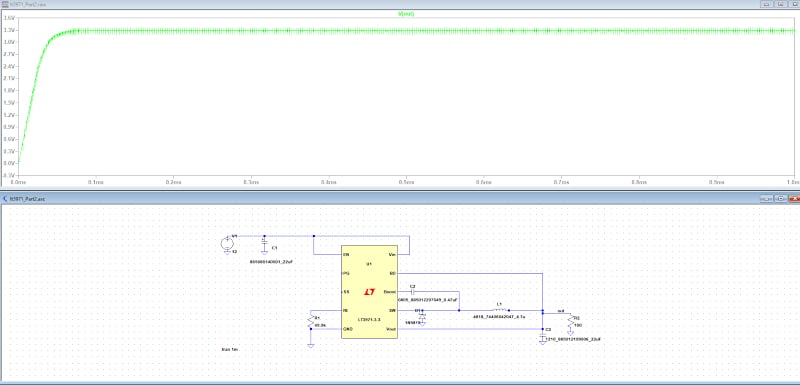
Figure 5. C3 is now a ceramic capacitor. The output is stable now, but if we compare this voltage output with the voltage output in Figure 2, we will notice the Vout is noisier now. Image used courtesy of Francesco Poderico
It already looks much better. However, not as perfect as we saw earlier.
Add the LISN and the power cable we designed in Part 3, and put it together.
The circuit becomes this:
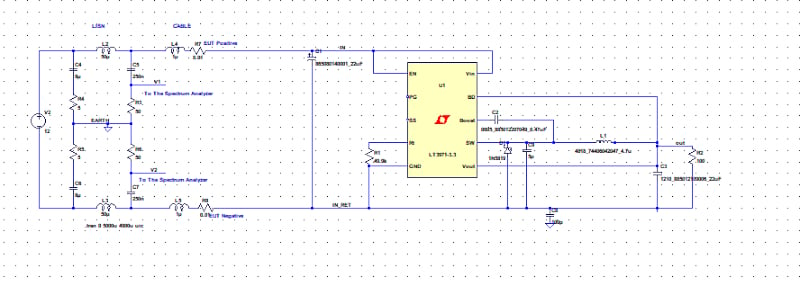
Figure 6. Adding a LISN and a 100 pF parasitic capacitor between the circuit return and the earth (see Part 1, Part 2, Part 3). Image used courtesy of Francesco Poderico
And the output voltage becomes this:
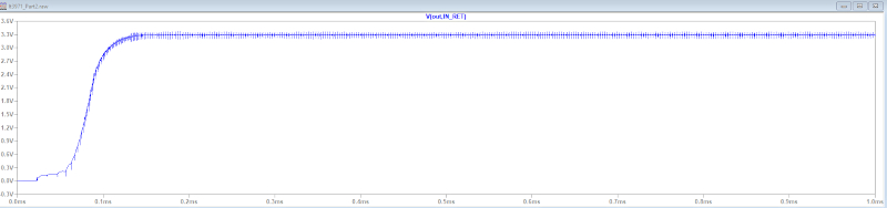
Figure 7. The Vout starts to look noisier now. Image used courtesy of Francesco Poderico
In Figure 6, you should notice a 5pF capacitor between the SW pin and U1 reference. I added those capacitors to emulate the internal Cds for the low-side MOS (inside U1), while C8 is the parasitic capacitor (100 pF) we studied in Part 3.
Common Mode and Differential Mode Noise
Now measure the common mode and differential mode voltage using the formulas we learned in Part 3.
VCM = (V1+V2)/2 [eq. 1]
VDM = (V1-V2)/2. [eq.2]
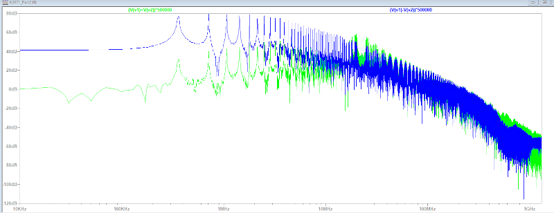
Figure 8. Common mode noise. Image used courtesy of Francesco Poderico
With LTSpice, it is possible to visualize the FFT of any signal or combination.
Since we are looking for the frequency response in dBuV, eq. 1 and eq. 2 need to be multiplied by a factor of 1,000,000. And so they become (V1+V2)*500000 and (V1-V2)*500000 (so it's in udBV already). If we imagine overlapping the EN55022 graph, we can already say that the emission is not too bad (please notice the load is only 100 ohm).
Reducing the Common Mode Noise
However, let's say we want to try to reduce the common mode noise. How can we do that?
We can add a CM choke, as shown below (L6).
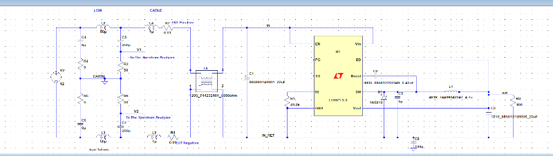
Figure 9. Adding a CM choke to improve the common mode noise. Image used courtesy of Francesco Poderico
Let’s see if the CM noise has changed now compared to the DM noise.
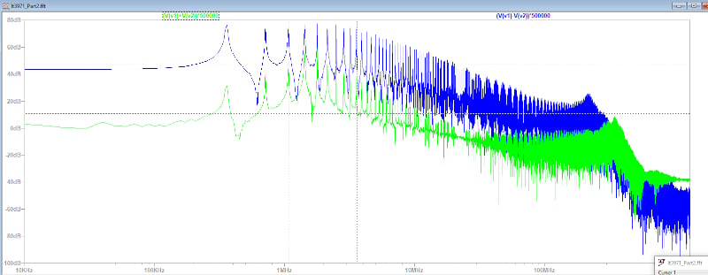
Figure 10. The common mode noise is now lower than in Figure 8. Image used courtesy of Francesco Poderico
Wow, what a difference. Now we can see a remarked separation between the common mode noise and the differential mode noise. After the insertion of L6, the differential mode noise has not changed drastically, but the differential mode noise had a remarkable reduction. L6 is still not the inductance I would have selected on a design because I have made a deliberate mistake... can you see it?
As an exercise, reduce the load R2 to get at least 0.5 A and then change L6, C1, and C3 to improve the emission. Good luck, and I hope you will be more confident to pass the CE now that you have a robust tool that allows you not to guess but select the proper components for the appropriate application.
Here are two more exercises.
Exercise 1: See what happens when you add in parallel to D1 a 47 pF capacitor in parallel to a 10-ohm resistor.
Exercise 2: See what happens when you add a resistor (1-10 ohm) in series to C2.
Featured image used courtesy of Adobe Stock