Facebook
 Google
 GitHub
 Linkedin
Designing Electronics to Pass the EMC Test Part 1
In Part 1, a systematic approach to minimize conducted emissions.
Every engineer should aim to design electronics to pass the Electromagnetic Compatibility (EMC) test the first time. However, that is easier said than done. Passing this test the first time is only possible if you understand how EMC testing is performed by an EMC house and the most common design techniques.
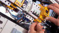
Exposing Your Design
When you do EMC testing, you expose all strengths and weaknesses of your design. I’m always present during the EMC testing because I know I will learn something new each time, and I strongly recommend you do the same. I use EMC testing as a tool to improve my skills and check my design for quality and robustness in different electromagnetic interference (EMI) scenarios.

Image used courtesy of EMC Fast Pass
˘¿This article will begin to cover Conductive Emission (CE) and will be divided into three parts:
- What is a CE test and why is it important?
- Typical Test setup for CE testing
- Designing techniques to prevent CE
What is CE Testing and Why Is it Important?
When we design an electronic product that has some form of switching (e.g., a microcontroller, an FPGA with one or more clocks, a DC/DC converter, etc.) chances are we will emit some kind of electromagnetic interference in the surrounding area. Those emissions may go from a few kHz up to several GHz. Emissions below 80 - 100 MHz, are most likely to use the cables as a medium of emission. This is the reason why the CE tests are usually carried up to 30 - 80 MHz (sometimes even higher), especially on power cables. This unwanted electromagnetic noise, if uncontrolled, may upset other equipment that shares the same power network – and this is the reason why it is so important.
Let's say, for example, we have designed a Joystick powered by a USB port and are injecting on the 5 V power bus a large noise due to some error in our design. Under some circumstances, the PC may not work correctly anymore. Imagine going to production and 10% of your joystick causes connected PCs not to work properly. It could damage the reputation of your company.
EMC testing is more than just an exercise in paperwork to get the FCC or CE mark. It is a way to prove that your product has the highest quality possible with today's technology.
Typical Test Set-Up
To understand the designing techniques needed to pass the CE one must first understand what is being measured, how it is being measured and the mechanism of emission. Once this becomes clear, what filter to apply, why to apply it and how to apply it can all be discussed.
The set-up for measuring CE changes slightly from standard to standard and application to application. For the sake of this discussion, our equipment uses the main AC line (220 V or 110 VAC) for power.
Then, an arrangement similar to the one drawn below will be set up from the EMC house. Your EUT (Equipment Under Test) will be placed on a table and connected to an LISN as shown in figure 1 below. The LISN is usually on the floor to maximize the CE loop. A LISN is a low pass filter that is placed between the AC line and the EUT and is used to create a controlled repeatable way to measure the emission. The LISN has one output signal (50 ohms) for the spectrum analyzer, which will scan all the frequencies starting from typically 9 kHz up to 30 MHz, 80 MHz.
For this test, the reference is not the earth but the ground reference you see in figure 1. The measurements will be done on both live and neutral.

Figure 1. A typical setup for conductive emission, the EUT is usually on a table 80 cm from the floor and 40 cm from the side (distances may change from standard to standard). Image used courtesy of Francesco Poderico
Now that we have learned what we are measuring some further questions need to be asked.
How is it possible that we have some RF noise from the setup above? Can we control it? What is the mechanism? The answer to these questions can be understood by looking at figure 2.
Imagine there is a sine wave generator inside the EUT. The RF emissions may couple on the ground planes placed near the EUT. This is one of the reasons why the EUT is so close to the vertical plane and why it is only 80 cm from the floor (during the test we are trying to maximize the coupling between the EEUT and the plate)
By looking at figure 2 again we can see in red a loop where the source is the sine wave inside the EUT and the loop is made by the two ground planes and the power cable.
We can see that:
- We can reduce the emission by reducing the coupling between the EUT and the two planes.
- We can reduce CE by adding a common mode filter on the power cable.
- We can reduce CE by adding X and Y capacitors, which will be discussed more in Part 2.

Figure 2. In the figure, we can see one of the reasons why the LISN is on the floor. It is to maximize the RF Loop. The EUT will emit some RF, some of them are coupled on the side plate and some are coupled to the floor. By having the LISN on the floor we maximize this loop. Image used courtesy of Francesco Poderico