Facebook
 Google
 GitHub
 Linkedin
Researchers Create ‘Perfect Crystal’ 2D Perovskites in Solar Cell
The metal halide perovskites had no distortions and outperformed other perovskites.
Bulk (3D) perovskite materials, which can produce high-performance solar cells, have been disrupting conventional silicon photovoltaic systems. However, while 3D perovskites get all the headlines, 2D perovskite materials are also improving the solar performance. Rice University researchers have created a 2D metal halide perovskite semiconductor that is close to being a “perfect crystal” at the atomic level.
These hybrid crystals feature a mixture of organic and inorganic constituents. Unlike fully inorganic semiconductors, these 2D materials have softer atomic lattices that are prone to distortion, so are less likely to form highly ordered and symmetrical crystal structures. Yet this latest research has transformed these 2D perovskites into a symmetrical lattice with no distortions.
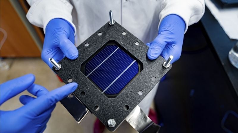
Solar cell with 2D perovskites. Image used courtesy of Rice University
What Are 2D Perovskites?
2D perovskites have a layered structure in which metal-halide layers are separated by organic cations, or “spacers,” that balance charge in the crystal structure. These spacers also separate the layers that define the 2D perovskite’s structure. The layer composition and spacer sizes change the optical and electronic properties of the 2D perovskite, allowing them to be tuned to the application.
2D and 3D perovskites differ in several ways. First, 2D materials have the structure of RAn-1BnX3n+1, where the metal halide layers form an octahedral BX6 structure. By comparison, 3D perovskites have the ABX3 structure.
Both structures are defined by:
- A = monovalent cation
- B = divalent heavy metal cation
- X = halide ions
- N = the number of perovskite layers between spacer layers
Beyond structural differences, 2D perovskites and 3D perovskites differ in features. 2D perovskites have higher thermal and moisture stability due to the spacers and a higher exciton binding energy than 3D perovskites, which creates more stable excitons.
Engineering More Effective 2D Perovskites
Rice University researchers created 2D perovskites without conventional distortions, enabling the fabrication of a highly symmetric material. They allow charge carriers to move through the crystal lattice with less impedance, losing less energy. As a result, more energy can be transferred when the sunlight hits the semiconductor junction.
The researchers explain their work. Video used courtesy of Rice University
The researchers stated that their material is as close as possible to perfect crystal symmetry, marking the first time this level of symmetry (and lack of distortion) has been achieved in multilayered 2D perovskite systems at room temperature.
The exciton transport performance of the 2D perovskite material outperformed other reported 2D perovskites and was comparable to that of monolayer transition metal dichalcogenides (TMDCs), another class of 2D materials with excellent semiconductor properties. The 2D perovskite had a short interlayer distance of 4 Å (Angstroms), a low optical bandgap of 1.7-1.8 eV, an exciton diffusion length of 2.5 µm, and a diffusivity of 4.4 cm2 s−1.
This performance improvement has been possible because the researchers prepared the 2D perovskites differently. Most synthetic approaches involve growing the perovskite crystal by allowing the reaction solution to cool. In this common method, the crystals grow on the reaction surface rather than staying in the bulk reaction liquid. However, the Rice researchers removed the crystals at a higher temperature before they had time to cool fully, locking in the desired symmetrical structure, rather than waiting for deformations to arise.
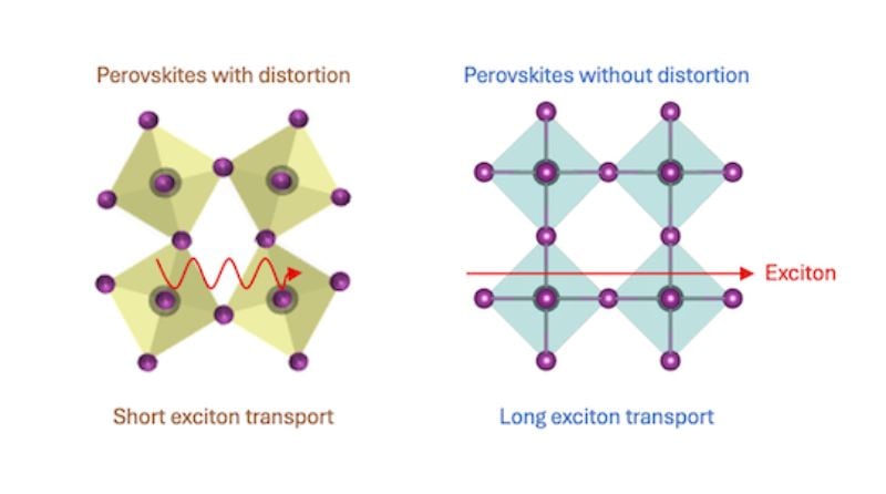
2D perovskite structure. Image used courtesy of Rice University/Jin Hou
In previous research, scientists have created thinner materials, but this new approach enabled the creation of thicker, multi-layered forms. It was also the first approach to connect more than two 2D perovskite layers in this configuration, using a formamidinium cation in between the metal halide layers.
Creating thicker 2D perovskites is beneficial for solar cell devices. As the material's thickness increases, its interaction with light changes. The greater the number of layers, the smaller the electronic bandgap in the semiconductor junction. The bandgap is the energy threshold required to absorb light, so a smaller bandgap allows the material to capture a larger portion of the solar spectrum: the more sunlight energy the cell can absorb, the better the solar cell’s performance.
The researchers stated that the bandgap is close to an ideal bandgap for pairing with both silicon and bulk perovskite solar cell junction materials.
Proof-of-Concept Device Shows Potential for Energy Boost
The researchers tested the 2D perovskite performance in a proof-of-concept self-powered photodetector. Photodetectors are highly sensitive light sensors that convert light into an electrical signal. They found that the photodetector based on their new 2D perovskite was more sensitive and had a faster response time than other 2D perovskites, showing its potential for applying it to solar cell technology (especially tandem solar cells), as well as other optoelectronic devices and quantum technologies.