Facebook
 Google
 GitHub
 Linkedin
Wide-Bandgap Perovskites for Tandem Solar Cells
Learn how stacking wide-bandgap perovskites with silicon solar cells may be an attractive option for increasing efficiency beyond single-technology solutions.
Globally, we’re seeing an increased demand for efficient and affordable solar energy. Researchers are increasingly looking beyond traditional silicon-based photovoltaics, which have long dominated the market. Silicon solar cells are quickly approaching their theoretical efficiency limits, leading to a surge of interest in tandem solar cells, which can harvest a broader spectrum of light by layering multiple materials with different bandgaps.
Among the most promising materials are wide bandgap perovskites, a class of hybrid semiconductors that can be tuned to efficiently absorb high-energy photons while transmitting lower-energy photons to underlying silicon layers. Despite promising lab results showing tandem silicon-perovskite cells with an efficiency exceeding 30%, the commercial viability of wide bandgap perovskites remains uncertain.
This article explores why wide bandgap perovskites have become central to the next generation of tandem solar technologies, and what work still needs to be done before they are widely adopted.
Perovskite solar cells. Image used courtesy of Adobe Stock
Why Wide Bandgap Perovskites Matter
Wide bandgap (WBG) perovskites are a subset of perovskite materials characterized by bandgap energies greater than 1.7 eV. This means they absorb high-energy photons at the blue end of the spectrum and convert them efficiently into electricity. This property makes them a good candidate for use as the top layer in tandem solar cells, where multiple photovoltaic layers with different bandgaps are stacked together to capture a broader range of the solar spectrum.
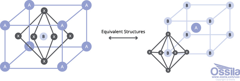
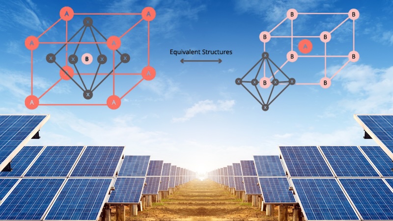
Example of a generic perovskite crystal structure of the form ABX3. Image used courtesy of Ossila
For example, in silicon-perovskite tandem architectures, WBG perovskites complement silicon’s lower bandgap (around 1.1 eV) by handling the high-energy portion of sunlight. The ideal bandgap for these top cells is around 1.7-1.8 eV, making WBG perovskites an obvious choice. This combination enables tandem devices to bypass the Shockley-Queisser limit (29% efficiency cap for single junction solar cells), with the theoretical efficiencies exceeding 40% in some designs.
Perovskite-silicon tandems are already demonstrating power conversion efficiencies (PCE) above 33%, significantly outperforming conventional silicon cells. Beyond just efficiency, perovskites have several other advantages that make them an appealing choice. WBG perovskites can be solution processed, have the potential for low-cost and scalable manufacturing processes, and have a composition that can be tailored, meaning that their bandgap can be tuned to match specific tandem configurations. Naturally, perovskites are hailed as one of the most promising materials for next-generation photovoltaics.
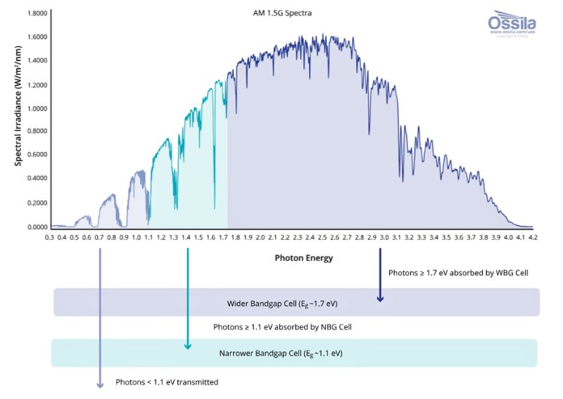
Light transmission through silicon-perovskite tandem solar cells. Image used courtesy of Ossila
Existing Issues With Perovskite
WBG perovskites show much promise, but their path to commercialization still faces many challenges. The biggest is instability, as these materials degrade rapidly under heat, moisture, and prolonged light exposure. When we consider that the intention is to use these materials in solar modules that are expected to withstand all kinds of weather for several years (over 20 years if they want to compete with silicon), the size of this issue becomes obvious.
This instability becomes a bigger problem considering that most high-performing perovskites contain lead. While the absolute amount of lead in a module is small compared to other industrial processes, degradation or improper disposal can still release toxic compounds into the environment. Alternatives, like tin-based perovskites, are being explored, but they currently suffer from even greater stability issues.
Another issue is phase segregation in mixed halide systems, typically iodine and bromide combinations, which tune the bandgap across a range of 1.5 to 2.3 eV. Under illumination and electrical bias, the halides undergo migration within the crystal lattice, causing phase segregation into iodine-rich and bromine-rich domains. This results in non-uniform bandgap regions, reducing the open-circuit voltage, short-circuit current, and the overall PCE.
What Research Is Being Done?
Much research is ongoing to address the inherent limitations of WBG perovskites. A particular focus area is triple-halide systems, a step further than mixed halide systems, where chloride is incorporated into the iodide/bromide mix to help mitigate phase segregation. Adding chloride helps to stabilize the lattice, reducing halide migration and improving bandgap uniformity.
For example, Xu et al. demonstrated a method to incorporate chloride, making it possible to create stable triple-halide perovskites with a bandgap of 1.67 eV. When integrated into two-terminal tandem silicon solar cells, this approach achieved a PCE of 27%, which is a significant step towards commercial viability.
Another focus area is compositional grading, which involves varying the distribution of halides across the film thickness to suppress segregation and improve stability. By creating graded homojunctions, researchers can better control electronic properties and reduce the energetic driving force for halide migration, improving operational stability and performance.
One of the biggest research areas is surface passivation strategies, which target defect states that act as non-radiative recombination centers. Because perovskites are typically solution-processed, defects such as vacancies and interstitials often form during crystallization. Passivation techniques are used to reduce the number of these defects through several methods, including introducing additives, forming 2D perovskite layers, or applying interfacial spacers. The goal is to make the perovskite more “passive,” meaning that it will interact less with its environment. Examples include coating fullerene derivatives onto the surface to reduce the trap density or using Lewis bases to fill vacancies. More advanced methods can use chelating agents such as F-PDI during solvent quenching and binding with lead at the grain boundaries.
What Happens With Perovskite Next?
WBG perovskites may become an important component of tandem solar cells, but taking them from the lab to market is still in the future. Beyond fundamental issues with the material, challenges must still be addressed to achieve batch consistency and high yield during manufacturing. While lab-scale devices have shown record efficiencies, producing uniforms that are defect-free across large areas is much more difficult. Minor variations, such as in composition or crystallinity, can drastically affect bandgap tuning, which is critical for tandem performance.
_with_transport_layer_(purple)_and_electron_transport_layer_(green)_in_a_perovskite_n-i-p_device.jpg)
Perovskite absorber layer (black) with transport layer (purple) and electron transport layer (green) in a perovskite n-i-p device. Image used courtesy of Ossila
Even if the technical challenges are solved, the issue of cost versus performance trade-offs remains. Today’s silicon-based photovoltaics are cheap, and the technology involved in the manufacturing processes is mature, owing to decades of research focused almost exclusively on making silicon solar cells the gold standard. Introducing WBG perovskite layers requires new deposition techniques and integration processes, often at high cost and low yield. These methods frequently involve controlled, contained environments to prevent moisture and oxygen exposure during fabrication. From an economic point of view, investment in this new technology is risky until clear roadmaps to manufacturing at scale become available.
So, what needs to happen next? Realistically, progress with WBG perovskites will be incremental rather than a sudden leap that changes the solar industry. Continued research into creating phase-stable compositions, along with developing new passivation strategies and deposition methods, will be the key to improving the reliability of these notoriously unstable materials. Simultaneously, hybrid approaches where WBG layers are integrated into existing silicon production layers could be the answer to cost-effective scaling.
Conclusion
Despite the challenges, there’s no denying that a big opportunity exists to change the solar industry's future. Tandem architectures with WBG perovskites have already demonstrated efficiencies exceeding 30%, and theoretical limits approach 40%.
If stability and scalability issues can be addressed, these materials could change photovoltaic economics within the next decade. In doing so, we could achieve a future with more energy generated from the same footprint, accelerating the transition to high-efficiency solar at scale.