Facebook
 Google
 GitHub
 Linkedin
Zero Overvoltage Switching
This article explains the zero overvoltage switching effect and gives insights into key aspects and applications.
Turning off an electrical path is causing trouble by parasitic inductance since the beginning of power electronics. Ages are spent to avoid oscillations and voltage overshoot while compromising on switching speed. Other research is focusing on low-inductive packaging technology, which is a good idea but will not finally eliminate parasitic inductance.
In contrast, the Zero Overvoltage Switching “ZOS” method offers a solution to unleash unlimited switching speed in real-world applications without overvoltage on the semiconductors. Moreover, in best case, it is even avoiding any subsequent parasitic oscillation. The idea is to use the intrinsic parasitic inductances and parasitic capacities to build up a resonant circuit. The turn-off event excites the resonant circuit and the free-wheeling diode stops it automatically after half a period, e.g. after a view nanoseconds. These resonant parasitic elements are thereby utilized to switch off a fixed current in a lossless, overvoltage free, and EMI compliant way. By designing the circuit and parasitics properly, there is no extra component necessary and even relaxed industrial style semiconductor housings and low-budget link capacitors can build up the circuit, as parasitic inductance is now a functional part of the topology.
Explaining the Zero Overvoltage Switching Effect
The technology focuses on the transistor turn-off event. To simplify the problem, the ZOS approach is described for a boost converter, as seen in Figure 1. In classic switching technology, the turn-off event is characterized by a specific turn-off switching time of the transistor Tbot, which causes the midpoint “MP” voltage to rise. To commutate the phase current IL from the transistor to the diode, an additional overvoltage occurs, forcing the current through the freewheeling path’s parasitic inductance Lpar. The amplitude of the voltage overshoot is given by the parasitic inductance, switching speed, parasitic capacities, and turn-off current.

Figure 1. Boost circuit
Not considered in this classic description is the freewheeling diode’s parasitic capacitance. While voltage at the midpoint is rising, a specific current starts to flow through Cpar,top. Turning off the transistor faster increases that current. When this current is large enough, the current commutation is done during voltage is rising, even without any voltage overshoot. The ZOS waveform has three steps:
- Step 1: The channel S inside the transistor turns off as fast as possible during t1, which may also take several ns in physical devices.
- Step 2: Phase current IPh charges the output capacity and thereby MP is rising. The parasitic top side capacity Cpar,top shifts the level of its cathode K over the DC link voltage UZK. Thereby current through Lpar rises and oscillation begins.
- Step 3: The oscillation ends immediately after half a period at t3, exactly where the current of Lpar is at its maximum. In an ideal setup, the maximum equals IPh while uD is zero at this point. Furthermore, the oscillator is stopped by the freewheeling diode, which simply shortens Cpar,top.

ZOS Cell Design
To convert the circuit into a ZOS Cell, the following design rules must apply. Figure 1 shows the parasitics, which are now part of the topology. The low side transistor Tbot is sketched as an ideal switch S next to additional (body-) diode and Cpar,bot and may represent a fast MOSFET for example.
-
The parasitic capacitance Cpar,top of the active free-wheeling component should be near or equal to the low side parasitic Cpar,bot. That is even true for typically non-linear capacities. This is easy to achieve in half-bridge configurations by default.
-
On a given hardware and parasitics, the phase current IPh at the turn-off point must be set according to following equation:
$$I_{Ph} = \frac{U_{ZK} \sqrt{8 \frac{C_{par}}{L_{par}}}}{\pi}$$
-
The chips and the gate driver design must turn off as fast and snappy as possible. That can be achieved e.g, by switching a 25 mΩ SiC MOSFET with a gate resistor RG of less than 1 Ω. Less speed will eliminate the ZOS effect.
Simulation Experiment
One ZOS showcase is a simulation experiment varying the gate resistance Rgate. Following classic theory, increasing the gate resistor lowers voltage overshoot. Following the rules of ZOS Cell design instead, overvoltage can be decreased against all expectations by lowering the gate resistance (and raising switching speed). By that approach, the simulated losses can be cut down to about 2 % of the nominal datasheet losses by applying an external Rgate of about 1 Ω additional to the internal chip resistance, instead of 20 Ω recommended. The simulation turns off the optimum ZOS current of 84 A using the 25 mΩ C2M0025120D Cree SPICE models with CPW41200S020B diodes parallel in half bridge configuration. The commutation loop inductance is 20 nH, link voltage is 800 V.

Figure 3. Voltage Overshoot in classic and ZOS Switching Technology
Measurement Experiment
Claiming overvoltage may disappear by increasing switching speed, adding parasitic inductance and ramp up the current is a very tough job resulting in disbelieve and shaking heads. That’s why a proof of concept test setup was build. The setup available has a drawback of 4,3 Ω gate resistors per chip while optimum would be below 1 Ω. To compensate this issue as far as possible, -10 V negative gate voltage (instead of -5 V) was applied to switch off faster.

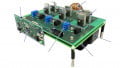
Figure 4. ZOS Test platform with module-integrated gate drivers, increased link inductance and film capacitors
The current IPh was alternated by changing the on-time and thereby ramp up different current values. Figure 5 shows a turn-off current of about 48 A. In Figure 6, an even larger current of about 68 A is turned-off, but parameters are hitting ZOS operation point.

Figure 5. Turning off a non-optimal current

Figure 6. Turning off the ZOS-optimized current
Channel 4 (green) shows the inductor current. Channel 2 (light blue) shows the voltage across the low-side transistor. Channel 1 (dark blue) is a trigger reference of the pulse generator input signal.
Further Key Aspects and Application
The key point of these rules is the unlimited switching speed, that allows cutting losses down to zero. Combined with classic Zero Voltage Switching (ZVS) during turn-on, it is possible to build up a real-world converter without significant switching loss at all.
Most applications need a power regulation. Several techniques allow set up average current while keeping optimum IPh at turn-off point:
- Switch off phases on multi-phase designs would allow NPh-step regulation.
- Under BCM operation, Valley Skipping can reduce power.
- Controlling power down to zero by burst-mode operation.
- Classic turn-off for small currents is still possible.
The ZOS technology can be used in every converter technology being able to control the current during the turn-off operation point. That is possible for nearly any classic isolated and non-isolated Buck-, Boost-, Forward-, Phase-shift, even Flyback- and other DC-DC converters from zero watts Point-of-Load converters to megawatt switching cells. Even load regulation is possible, implementation is more easy for constant-power applications like LED illumination or on-board chargers.
About the Author
Dipl.- Ing. Stefan Matlok studied Mechatronics at the Friedrich Alexander University Erlangen majoring in power electronics. Since 2011, he specialized on switching circuit designs and develops FPGA and μC control boards for high power traction converters. As head of the DC/DC converter group at the Fraunhofer IISB, he works on new prospects improving functional features, power density, EMI, efficiency, and digital control techniques.
This article originally appeared in the Bodo’s Power Systems magazine.