Facebook
 Google
 GitHub
 Linkedin
Revolutionizing Power Electronics: GaN Bidirectional Switches
Unidirectional switches (UDS) have long served power conversion systems, but they come with inherent limitations. A bidirectional GaN switch approach offers many advantages.
This article is published by EEPower as part of an exclusive digital content partnership with Bodo’s Power Systems.
Article co-authored by Dr. Kennith Kin Leong, Lead Principal, Product Definition and Concept Engineer, High-Voltage GaN Bidirectional Switch at Infineon Technologies.
Limitations of Traditional Approaches
For years, engineers have grappled with the fundamental constraints of unidirectional switches. When bidirectional voltage blocking is required, designers must implement back-to-back configurations using multiple discrete components, leading to increased system complexity, larger footprints, and higher costs. These arrangements also introduce additional parasitic elements that compromise switching performance and efficiency. Furthermore, traditional three-terminal UDS devices lack the flexibility to control current flow in both directions independently, limiting their applicability in advanced power conversion topologies.

Image used courtesy of Adobe Stock
These challenges have become increasingly significant as the industry pushes toward higher power density, greater efficiency, and reduced system costs. The conventional approach of using back-to-back discrete switches in applications such as Vienna rectifiers, T-type converters, and HERIC configurations results in suboptimal designs that fall short of meeting evolving market demands. This has created a pressing need for innovative solutions that can overcome these fundamental limitations while delivering enhanced performance across a wide range of operating conditions.
Introducing the CoolGaN Bidirectional Switch (BDS) Family
To address these challenges, Infineon has pioneered a groundbreaking solution: CoolGaN Bidirectional Switch (BDS) 650 V G5. This innovative device family represents a paradigm shift in power switch technology, offering unprecedented control and flexibility for next-generation power conversion systems. Unlike conventional approaches that require multiple discrete components arranged in back-to-back configurations, it provides a monolithic solution capable of actively blocking voltage and current in both directions.
Infineon’s CoolGaN Bidirectional Switch portfolio caters to a wide range of voltage requirements. With the 650 V portfolio housed in TOLT and DSO packages, and 850 V options available soon, the company also offers lower voltage options, starting from 40 V. These lower voltage GaN switches are used in consumer electronics, where they serve as battery disconnect switches.
CoolGaN BDS 650 V G5 features a revolutionary common drain design with a double gate structure, leveraging Infineon’s proven rugged Gate Injection Transistor (GIT) technology. This unique architecture enables the use of the same drift region to block voltages in both directions, resulting in a significantly reduced die size compared to conventional back-to-back arrangements. The compact, integrated design not only saves space but also minimizes parasitic elements, enabling faster switching speeds and improved efficiency.
Technical Innovation: Four-Quadrant Operation
What truly sets the high-voltage CoolGaN BDS family apart is its unprecedented four-quadrant control capability. Unlike traditional three-terminal unidirectional switches, the BDS features four active terminals plus an additional substrate terminal. This configuration enables four distinct modes of operation: two traditional ON/OFF modes and two diode modes, providing designers with an unprecedented level of control flexibility.
In the bidirectional OFF mode (switch mode OFF), the device blocks voltage in both directions when zero or negative voltage is applied to both gates, effectively functioning as an open circuit. Conversely, in the bidirectional ON mode (switch mode ON), current can flow freely in both directions when both gates are activated, similar to a standard MOSFET in the on-state. These modes alone provide significant advantages over conventional solutions, but the true innovation lies in the two additional diode modes.
The diode modes—reverse blocking (RB) and forward blocking (FB)—allow the BDS to selectively block voltage in one direction while permitting current flow in the opposite direction. In diode mode RB, the device blocks voltage from bottom to top but allows current flow from top to bottom. Conversely, in diode mode FB, it blocks voltage from top to bottom while allowing current to flow from bottom to top.

Figure 1. The four modes of operation and ten possible transitions of the CoolGaN Bidirectional Switch 650 V G5, highlighting its unique capabilities and flexibility. Image used courtesy of Bodo’s Power Systems [PDF]
These modes are particularly valuable for soft-switching operations where the voltage blocking direction is known, ensuring safe discharge of output capacitance and optimal performance.
Engineering Excellence: Integrated Substrate Voltage Control
A significant technical challenge in designing CoolGaN BDS was managing the substrate voltage. In traditional UDS designs, the substrate is typically tied to the source to prevent back-gate effects that reduce 2DEG (two-dimensional electron gas) charge concentration. However, the common drain configuration of the BDS, with its two sources, made this approach impractical. Simply floating the substrate would lead to uncontrolled potential and detrimental back-gate effects.
To overcome this challenge, Infineon developed an innovative monolithically integrated substrate voltage control circuit. This ingenious solution dynamically connects the substrate to the source with the lowest potential, ensuring optimal performance without requiring external support circuitry. This integrated approach enables the BDS to operate effectively in both soft and hard switching modes, adapting to various application requirements for optimal performance and efficiency.
Performance Characteristics: Data-Driven Excellence
CoolGaN BDS demonstrates exceptional performance across a wide range of operating conditions. One of the key parameters for evaluating its performance is the source-to-source resistance (Rss(on)), which directly impacts conduction losses and overall efficiency. The static Rss(on) approximately doubles as the temperature varies from 25°C to 150°C (Figure 2), highlighting the importance of temperature considerations in system design. Notably, unlike some SiC MOSFETs that may exhibit a negative temperature coefficient at low temperatures, CoolGaN BDS maintains a positive coefficient even down to -40°C, ensuring reliable operation across its entire temperature range.
Adjusting the steady-state gate current can optimize Rss(on) by up to 3%, improving performance at the cost of higher gate current loss. Additionally, increased gate current can boost saturation current by 60% or more, balancing efficiency and performance in system design.
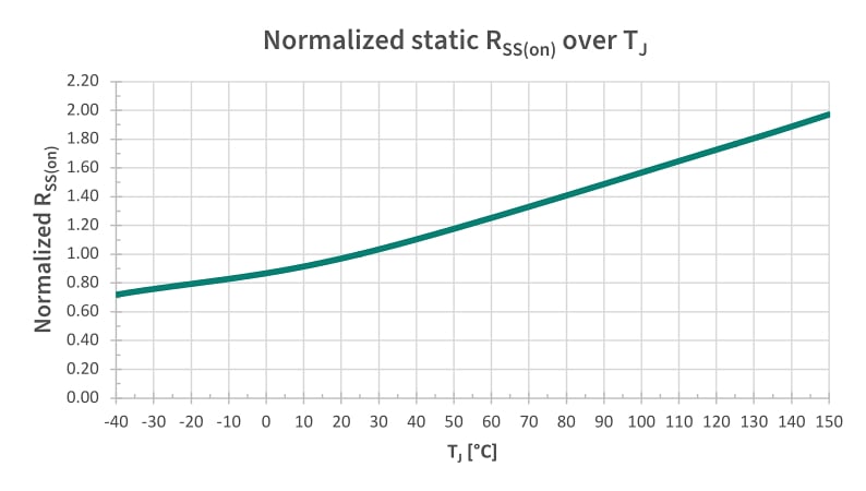
Figure 2. Normalized Rss(on) value of the CoolGaN BDS across the entire operational temperatures. Image used courtesy of Bodo’s Power Systems [PDF]
Dynamic Rss(on) provides a realistic measure of the performance of CoolGaN BDS during continuous switching, influenced by blocking voltages, switching frequencies, and temperature. A modified selfcompensated double diode drop On-state Voltage Measurement Circuit (OVMC) was used in a boost converter setup with the BDS as the low-side switch and a high-side SiC Schottky diode in Continuous Conduction Mode (CCM).
At 50 kHz and 100 kHz hard switching, dynamic Rss(on) remained close to its static value, with only a 5-7% increase. Higher frequencies increased dynamic Rss(on) due to shorter measurement periods. Temperature also affected dynamic Rss(on), but CoolGaN BDS showed stable performance across typical conditions, ensuring predictable behavior in end applications. This stability highlights the device’s robust design, making it suitable for high-frequency and thermally demanding environments.
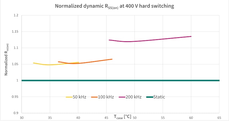
Figure 3. Normalized dynamic Rss(on) with different switching frequencies over case temperatures. Image used courtesy of Bodo’s Power Systems [PDF]
The soft-switching performance is even more impressive, as depicted in Figure 4. At 110 V, 500 kHz, the dynamic Rss(on) is approximately 5% higher than the static value, while at 400 V, it rises by roughly 16.5%. This variation with AC grid voltage suggests that using the AC voltage as an average value across the cycle is a practical approach for system design optimization. Moreover, even as switching frequencies increase from 100 kHz to 300 kHz, the normalized dynamic Rss(on) rises only marginally to 1.06 or by just 6% (see Figure 5), highlighting the benefits of soft switching in minimizing the impact of frequency on performance.

Figure 4. Normalized dynamic Rss(on) with different blocking voltages at 500 kHz over case temperatures. Image used courtesy of Bodo’s Power Systems [PDF]
Figure 5 shows the normalized dynamic Rss(on) for CoolGaN BDS under soft switching at 400 V against case temperatures. At 100 kHz, dynamic Rss(on) is approximately at 1 with static value and rises slightly with frequency, reaching only 1.06 at 300 kHz. This minimal increase highlights the benefits of soft switching in minimizing frequency impact and enhancing efficiency.

Figure 5. Normalized dynamic Rss(on) with different switching frequencies at 400 V input over case temperatures. Image used courtesy of Bodo’s Power Systems [PDF]
Switching Losses: Precision Measurements
Accurately determining switching losses is crucial for evaluating the efficiency of wide-bandgap devices like CoolGaN BDS. Currently, there is no known method to accurately separate turn-on and turn-off losses for the BDS. While soft-switching losses are very low, turn-on losses are not zero due to contributions from the substrate voltage control circuit and Coss hysteresis losses. Consequently, all switching losses are expressed as switching loss per cycle in microjoules, encompassing both turn-on and turn-off losses.
For hard-switching measurements (Figure 6), a boost setup operating in Continuous Conduction Mode (CCM) was employed, with conduction losses deducted from calibrated thermal losses. Testing at 500 kHz revealed losses scaling proportionally with turn-off current and input voltage.

Figure 6. Hard-switching losses per cycle for CoolGaN® BDS 650 V G5 (IGLT65R055B2) at 500 kHz at two different input voltages. Image used courtesy of Bodo’s Power Systems [PDF]
Soft-switching evaluations (Figure 7) used a half-bridge configuration in triangular current mode across three voltage levels (110 V, 240 V, and 400 V), demonstrating significantly reduced losses compared to hard switching. This comprehensive per-cycle data enables designers to accurately predict thermal requirements and optimize efficiency in practical applications, despite the inability to isolate individual switching events.

Figure 7. Soft-switching losses per cycle for CoolGaN BDS 650 V G5 (IGLT65R055B2) at 500 kHz at three different input voltages. Image used courtesy of Bodo’s Power Systems [PDF]
Design Considerations: BDS vs. Back-to-Back (B2B) Comparison
When evaluating CoolGaN BDS, it is essential to compare them against traditional back-to-back (B2B) configurations and not against a single UDS.
CoolGaN BDS demonstrates a superior Figure of Merit (FoM) compared to Si and SiC B2B configurations, offering over 85% lower Rss(on) × QG. This results in significantly lower energy losses per cycle, making it ideal for high-frequency applications.

Figure 8. FOM comparison of BDS and B2B configurations by technologies. Image used courtesy of Bodo’s Power Systems [PDF]
Gate Driving and Supplies
CoolGaN BDS is a common drain device featuring two gates controlled in reference to its own source, each with its own kelvinsource terminal for the return path of the gate drives. This BDS uses the GIT technology, which requires an RC interface for each gate to control the turn-on and steady-state gate current gate.
A key benefit of the RC interface is its ability to generate a natural negative gate voltage during turn-off, a recommended practice for all discrete GaN switches. For the BDS, each gate requires its own isolated gate driver as well as an isolated auxiliary supply. Although the total number of auxiliary supplies depends on the specific circuit topology, some nodes can share a common supply.
Gate Driving
Infineon offers a comprehensive portfolio of EiceDRIVER Gate Driver ICs with a variety of isolation levels, voltage classes, protection features and packages. The ICs are available in single channel configurations, as shown in Table 1.
| Product code | Isolation type | Configuration |
| 1EDB7275F | Basic | Single channel |
| 2EDB7259Y | Basic | Dual channel |
| 2EDR7259X | Reinforced | Dual channel |
Table 1. EiceDRIVER Gate Driver ICs
These driver ICs form the optimal combination with CoolGaN BDS to achieve high efficiency, robustness, and power density in high performance applications. Visit www.infineon.com/gatedrivers for more information about EiceDRIVER product families and available evaluation boards.
Isolated Auxiliary Supply
Creating an isolated auxiliary supply for CoolGaN BDS can be achieved through various methods, each with its own trade-offs. The straightforward approach of small, isolated DC-DC modules is a costly option. A more cost-effective alternative is to design an isolated auxiliary supply directly on the PCB using pulse transformers.
Although this may consume more PCB space, this pulse transformer approach reduces the costs of an isolated auxiliary supply while providing a high degree of flexibility and customization. By leveraging the 1EDN7512G driver IC and a pulse transformer, designers can create a compact and efficient isolated auxiliary supply that meets the specific needs of their application.
Transforming Applications: Practical Benefits
CoolGaN BDS is poised to revolutionize a wide range of applications, offering significant advantages over conventional solutions. One of the most immediate benefits is the ability to replace backto-back discrete switches in existing designs. In applications such as Vienna rectifiers, T-type converters, and HERIC configurations, the BDS provides a more integrated, efficient, and cost-effective solution.
Perhaps even more exciting is the potential to enable single-stage DC/AC conversion in solar micro-inverters and other single-stage isolated topologies. By allowing bidirectional voltage blocking in a single device, the BDS simplifies circuit designs, reduces component count, and enhances efficiency. This leads to more compact, cost-effective solutions that are quicker to bring to market, providing a competitive edge in today’s fast-paced industry.
The single-stage isolated AC power conversion application demonstrates several key advantages: improved efficiency through fewer conversion stages, reduced sizes, and lower costs with the use of high-frequency transformers. Additionally, it also shows enhanced flexibility enabling voltage scaling, frequency conversion, and natural bidirectional power flow. While challenges such as switching losses, EMI, control complexity, and component stress must be addressed, CoolGaN BDS provides the foundation for overcoming these obstacles and developing next-generation power conversion systems.
Conclusion: Pushing the Boundaries of Power Electronics
CoolGaN BDS 650 V G5 represents a significant leap forward in power switch technology, addressing long-standing challenges and opening new possibilities for power conversion system design. By integrating bidirectional blocking and conduction capabilities into a single monolithic device, it reduces component count, simplifies design, and enhances performance across a wide range of applications.
The innovative four-mode operation, combined with the integrated substrate voltage control circuit, provides unprecedented flexibility and control for next-generation power systems. The exceptional performance characteristics, meticulously quantified through advanced measurement techniques, enable designers to accurately predict and optimize system behavior in real-world applications.
As the power electronics industry continues to push for higher efficiency, greater power density, and reduced costs, CoolGaN BDS stands as a testament to Infineon’s commitment to innovation and engineering excellence. By challenging conventional approaches and developing groundbreaking solutions, Infineon is not just addressing today’s design challenges but also laying the foundation for tomorrow’s power conversion systems.
For design engineers looking to stay at the forefront of power electronics technology, CoolGaN BDS offers a compelling solution that combines technical innovation with practical benefits. Whether you are designing solar inverters, power supplies, motor drives, or other power conversion systems, this revolutionary technology provides the tools you need to create more efficient, compact, and cost-effective products that meet the demands of today’s market while preparing for the challenges of tomorrow.
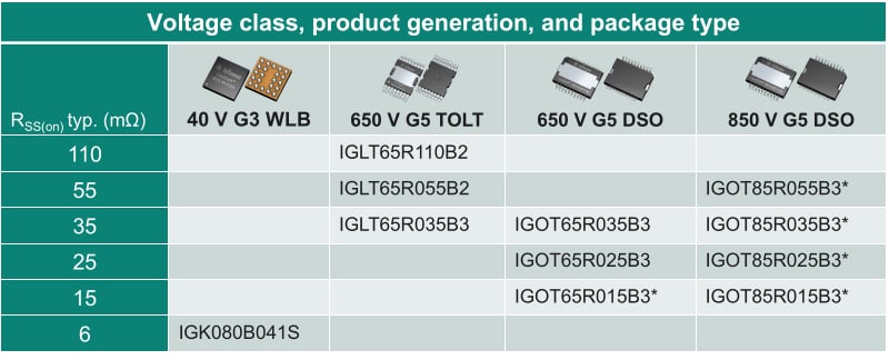
Figure 9. CoolGaN Bidirectional Switch (BDS) 2025 portfolio; * indicates products in the roadmap. Image used courtesy of Bodo’s Power Systems [PDF]
Discover more about CoolGaN BDS 650 V G5 on www.infineon.com/gan-bds-hv and see how this cutting-edge solution can revolutionize your next project. The future of bidirectional switches is here, and it is CoolGaN BDS.
This article originally appeared in Bodo’s Power Systems [PDF] magazine and is co-authored by Natascia De Patre, Manager, Product Marketing, High-Voltage GaN, and Dr. Kennith Kin Leong, Lead Principal, Product Definition and Concept Engineer, High-Voltage GaN Bidirectional Switch, both Infineon Technologies.