Facebook
 Google
 GitHub
 Linkedin
Why Do Switching Transistors Fail?
This article examines practical experiences and explains why switching transistors fail based on a flyback converter.
This article is published by EEPower as part of an exclusive digital content partnership with Bodo’s Power Systems.
Overvoltage on the switching transistor is the most frequent cause of failure in my fault analyses. This has not changed in the last 25 years, although today’s MOSFETs should be much more robust than earlier bipolar transistors. Many MOSFETs have an avalanche energy rating. In the event of an overvoltage, they do not fail immediately, but the specified amount of energy must first be exceeded before the avalanche effect is triggered.
Image used courtesy of Adobe Stock
For many switching power supply developers, this seems to be a great feature because they no longer have to look so closely at the voltage peaks. Whether at maximum mains voltage, during start-up, or in the event of a short circuit, if the energy of the overvoltage is significantly below the specified datasheet value, you can proceed with blind confidence. That could be a fatal mistake.
From Where Does the Overvoltage Come?
The culprit is clear and easy to identify: it is the parasitic inductance Lleakage, which is not demagnetized via the freewheeling diode D2 during the transfer time. The energy stored in it (½ Lleakage I2) is transferred to the existing parasitic capacitance and generates an overvoltage there (½ CparasiticV2). If there were no parasitic capacitance, the voltage would rise to infinity. The resultant MOSFET voltage is greatest in the flyback converter (Figure 1) because the overvoltage is superimposed on the shoulder voltage.
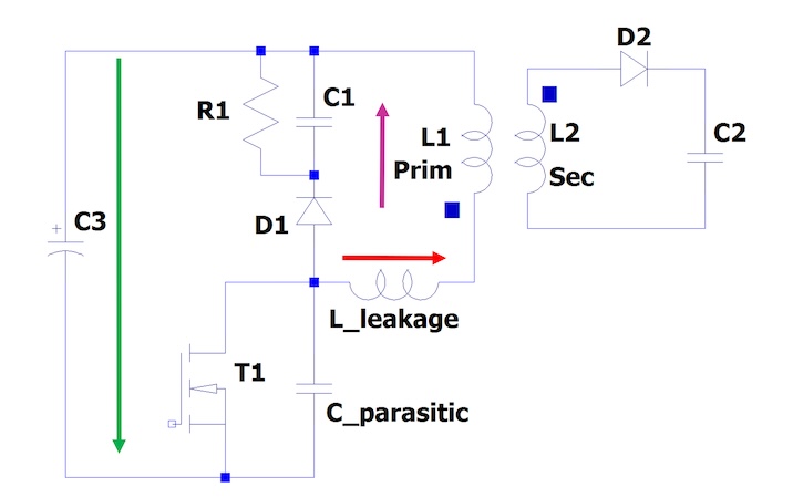
Figure 1. Flyback converter principle with leakage inductance and R-C-D snubber network. Image used courtesy of Bodo’s Power Systems [PDF]
Due to the air gap in the transformer and the freewheeling diode situated on the secondary side, the leakage inductance is very high with this topology. The junction capacitance of the switching transistor is low, resulting in a high overvoltage peak (Figure 2). However, regardless of the topology, there is always some leakage inductance due to the leads and vias.
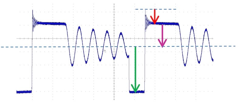
Figure 2. Typical drain voltage curve on the switching transistor of a flyback converter. Image used courtesy of Bodo’s Power Systems [PDF]
How Do You Measure Overvoltage Correctly?
It is difficult to measure this overvoltage peak correctly because it is reduced by the effect of the probe capacitance. In addition, the peak is sometimes only a few nanoseconds long, and the properties (bandwidth, resolution, memory depth) of the overall probe and oscilloscope system are often insufficient. It is interesting to note that measurements made by three different engineers using their own equipment on the same power supply yielded drain voltage values between 710 V and 850 V. In the case of a 750 V MOSFET, this can be the difference between life and death.
Do You Need a Snubber Network?
We only measure a power supply sample at room temperature. The overvoltage peak depends on parasitic element properties whose values are poorly specified and which also have large tolerances and are temperature dependent. For this reason, a snubber on the switching transistor is recommended to mitigate fluctuations occurring in production quantities. For the flyback converter, I consider a classic R-C-D snubber (Figure 1) the optimum solution in terms of reliability. The capacitor absorbs the energy of the leakage inductance, the resistor discharges it for the next cycle, and the diode ensures a low-impedance circuit in the charge direction and brings the resistance into the circuit in the discharge direction to minimize losses in the switching transistor when it is switched on. That means the snubber diode serves as a freewheeling diode for the leakage inductance and should therefore be as close as possible to the drain of the MOSFET. Alternatively, you could use a single capacitor, an R-C element, or a robust TVS diode that absorbs the voltage spike. Unfortunately, a snubber costs money and space and increases power losses.
What Do Avalanche Energy and Avalanche Current Mean for MOSFETs?
If an overvoltage occurs in the semiconductor, the first electron is knocked out of its bond and this knocks out further electrons. This leads to an avalanche effect which destroys the component. For MOSFETs with an avalanche energy rating, a certain energy threshold must first be exceeded before the avalanche effect is triggered. This energy is specified in the datasheet of a MOSFET.
In the case of the ST45N65, the avalanche energy rating is exactly 810mJ at a junction temperature of 25 °C (Figure 3). This value is, of course, completely irrelevant. Which switching transistor is operated at 25 °C? The avalanche energy at 110 °C would be far more pertinent. This is important to know but is not specified in the datasheet.
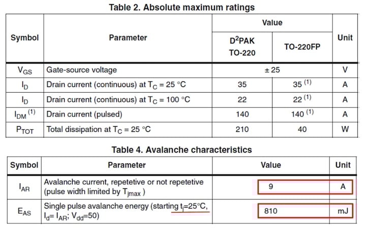
Figure 3. Extracts from the STF45N65 datasheet. Image used courtesy of Bodo’s Power Systems [PDF]
This MOSFET from ST can pulse 140 A and yet the avalanche current is specified as 9 A (Figure 3). The current is the same in the main inductance and leakage inductance, and it continues to flow into the MOSFET after it is switched off. Who operates a 140 A MOSFET at 9 A?
Infineon specifies this better. In the 600 V CoolMOS datasheet for the IPL60R185P7, the avalanche energy is specified as a function of temperature (Figure 4).
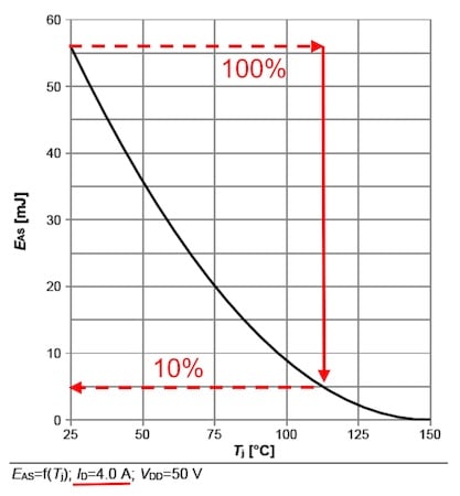
Figure 4. Avalanche energy as a function of the junction temperature (datasheet extract IPL60R185P7). Image used courtesy of Bodo’s Power Systems [PDF]
The graph shows that at a junction temperature of 110 °C, only 10 % of the original value of 25 °C remains, i.e. only 5 mJ instead of the original 55 mJ.
Unfortunately, the MOSFET temperature can only be measured outside the housing and integrated over time. In fact, the actual temperature on the chip pulses with the switching frequency depends on the switch-on, conduction, switch-off losses, and the transient thermal impedance. This can be simulated with LT-Spice, for example. Therefore, we do not know exactly how high the chip temperature is when the overvoltage pulse occurs. In any case, it is higher than measured at the housing. When the MOSFET blocks, the junction cools down. If we have zero voltage switching, then there are no switch-on losses. As soon as the current flows, the conduction losses increase quadratically with the current (I2 x RDSon), and the chip heats up quickly. There are large switch-off losses when switching off, and the chip becomes hot. This is precisely when the overvoltage peak occurs and when we must know the junction temperature to read off the avalanche energy still permitted in the diagram.
According to its datasheet, this power MOSFET from Infineon can handle a pulse current of 53 A. So, it will probably not be operated with only 4 A. However, according to the small print on the left below the diagram, the avalanche energy is precisely specified with a value of 4 A (Figure 4). The maximum permissible avalanche current is also specified as 4 A in the datasheet (Figure 5). This means we should not operate the 53 A MOSFET with more than 4 A if we want to utilize the avalanche energy, which only applies at 25 °C.
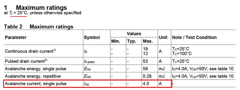
Figure 5. Maximum ratings (datasheet extract IPL60R185P7). Image used courtesy of Bodo’s Power Systems [PDF]
In the case of avalanche energy, we have seen that at 110 °C, only 10 % of the value of 25 °C is permitted. Unfortunately, there is no diagram showing the Avalanche current as a function of temperature. We can only hope that the derating is not 10 % at 110 °C, as with the avalanche energy; otherwise, only 400 mA would be permitted.
How Do MOSFET Manufacturers Specify Avalanche Energy Ratings?
Let’s look at how almost all MOSFET manufacturers measure and determine the avalanche energy, using Infineon as an example. Before the test, the MOSFET is connected to 50 V via the coil and free from stress at 25 °C. In the real power supply unit, the MOSFET is at 300 V to 400 V before switching on and at 500 V in the off state, so you already have leakage currents of up to almost 1 mA and corresponding losses. In addition, the MOSFET in the power supply unit constantly switches currents on and off at a high frequency, and its temperature might be 100°C or higher.
In the test, however, the MOSFET is only switched on once and allowed to conduct until the specified current (e.g., 4 A) is reached. The test circuit (Figure 6) is similar to a boost converter but without a freewheeling diode to demagnetize the inductance. As soon as the MOSFET switches off, the drain voltage increases indefinitely and is only clamped by the MOSFET to a value V(BR)DS that is somewhere above the maximum permissible reverse voltage. This can often be seen when measuring a plateau that suddenly limits the oscillation. In the test, the MOSFET remains off forever and is at 50 V.
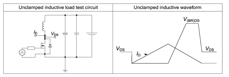
Figure 6. Datasheet extract for the avalanche energy test. Image used courtesy of Bodo’s Power Systems [PDF]
In an application note from Infineon on the subject of avalanche energy, you can see an oscilloscope diagram (Figure 7), which shows that the MOSFET conducts for 40 µs (current ID rises) and demagnetization takes 22 µs (current ID falls). The avalanche energy, therefore, has 22 µs to distribute itself in the chip.
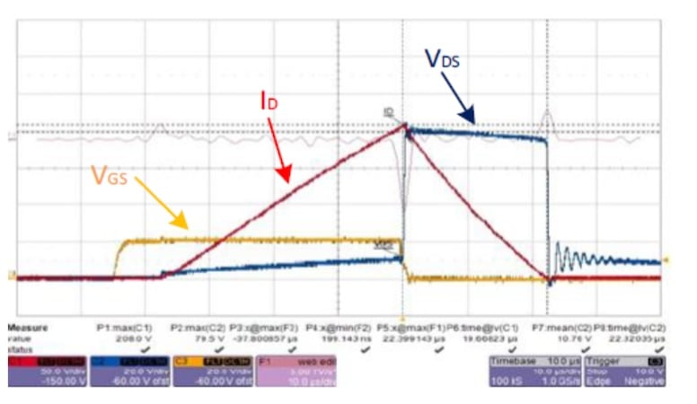
Figure 7. Datasheet extract for the avalanche energy test. Image used courtesy of Bodo’s Power Systems [PDF]
In an application note from Vishay, I read another interesting aspect (Figure 8): “Typical modern power MOSFETs have millions of identical trenches, cells or many strips in parallel to form one device...For robust designs, then, the avalanche current must be shared among these cells/strips evenly.”
Typical modern power MOSFETs have millions of identical trenches, cells or many strips in parallel to form one device, as shown in figure 7. For robust designs, then, avalanche current must be shared among many cells/strips evenly.
Figure 8. Extract from an application note from Vishay. Image used courtesy of Bodo’s Power Systems [PDF]
In this Vishay application note, there is also an oscillogram showing the demagnetization of the inductance; thus, the overvoltage lasts 70 µs.
Durations of 22 µs or 70 µs are irrelevant—the overvoltage in the power supply lasts a tiny fraction of those times, between 5 ns and 500 ns. The avalanche current must, therefore, be distributed evenly across the millions of parallel structures in a hundredth to a thousandth of the time specified in the datasheet to achieve a “robust design.” This means that the chip-internal resistors and inductances play a major role. As far as I know, MOSFET manufacturers do not test this scenario – and if they don’t test it, there is a strong chance they won’t optimize the design for it either.
In addition, there are often many voltage peaks in succession, whether during start-up, mains interruption, mains surge voltage, or in the event of an overload or short circuit. In some datasheets, the repetitive value can also be found alongside Single Pulse Avalanche Energy. For the Infineon CoolMOS device (Figure 5), the repetitive value is only 5% of the single pulse and has the same unrealistic test conditions.
The avalanche energy datasheet often specifies gate voltage zero as a condition. Take a close look at your oscilloscope measurement: During the voltage peak on the drain, the gate voltage is often clearly positive, one volt or more, due to the miller effect and an imperfect gate driver circuit.
Consider or Ignore Avalanche Energy?
Based on these findings and considerations, the question arises as to whether the specified avalanche energy should be considered. The answer is a clear “no” for me. The maximum permitted drain voltage applies, which must not be exceeded in any operating case. This is an important prerequisite for getting a reliable power supply unit.
The MOSFET manufacturers say the same thing: The maximum ratings must be strictly adhered to, even for short torques, because, otherwise, the service life and reliability of the MOSFET cannot be guaranteed.
We power supply developers test our circuit; if nothing breaks, we give it the thumbs up. But if only 100 of these millions of parallel structures break, we won’t even notice. The quality department may carry out a thousand tests, but even then, we don’t notice that a hundred thousand structures are broken because there are still millions intact. There’s a lot of guesswork when the customer’s device fails a year or more later, everything has been calculated and tested and found to be good.
Recommendations
The maximum reverse voltage of a MOSFET is specified in the datasheet. Many MOSFET manufacturers warn against exceeding this maximum permissible reverse voltage, even briefly, so as not to impair the service life and reliability.
If an avalanche energy is specified in the datasheet, then this will not correspond at all to the real application in the switching power supply. The avalanche current is much higher, the temperature is much higher, and the overvoltage peaks will always be repetitive. In addition, the avalanche energy in the power supply must be distributed evenly over the millions of parallel structures in the chip in a thousandth of the time specified by the MOSFET manufacturer. It doesn’t help if some manufacturers test 100 % of the avalanche energy in production. Even extensive long-term testing in the power supply unit only provides deceptive certainty because the semiconductor may only be damaged a little more with each test and then only fail at the customer’s premises after a year of operation.
My recommendations:
1. Stay below the maximum specified reverse voltage in all operating conditions.
2. The more uncertain you are about the accuracy and reproducibility of your measurement, the more margin you should allow.
These recommendations apply not only to switching transistors in AC/DC converters on the primary side but also to synchronous rectification on the secondary side, half bridges in DC/DC converters, and Schottky diodes with avalanche ratings.
This article originally appeared in Bodo’s Power Systems [PDF] magazine and is co-authored by Professor Markus Rehm, who runs a power electronics laboratory, and Sean Carthy, owner of consultancy InducAce Ltd.