Facebook
 Google
 GitHub
 Linkedin
Boost Inverter Efficiency by Decoupling Switching Losses and Switching Speeds
Learn how researchers at FAU Erlangen-Nürnberg, in collaboration with Sanan Semiconductor, have developed a soft-switching inverter that achieves efficiencies exceeding 99.6%.
Article co-authored by Thomas Lehmeier, Yan Zhou, Institute of Power Electronics, and Ajay Poonjal Pai, Head of WBG Semiconductor Innovation, Munich, Sanan Semiconductor.
This article is published by EEPower as part of an exclusive digital content partnership with Bodo’s Power Systems.
Soft-switching power inverters can resolve the traditional trade-off between minimal switching losses and switching speeds. Researchers at FAU Erlangen-Nürnberg, in collaboration with Sanan Semiconductor, have developed a soft-switching inverter that achieves efficiencies exceeding 99.6%. This advancement enables EV manufacturers to improve the driving range and fully utilize the capabilities of wide-bandgap semiconductors.
Why Aren’t We Exploiting the Full Potential of Wide-Bandgap Semiconductor Devices?
High efficiency, low cooling effort, and compact passive components are essential goals for modern power electronics. Wide-bandgap semiconductor materials, such as silicon carbide (SiC) and gallium nitride (GaN), present new opportunities to meet these requirements. While the higher switching speeds enabled by SiC and GaN transistors allow for lower losses, and therefore, more compact power electronic systems, they also result in higher dv/dt stresses on the motor windings. To mitigate these effects, practical designs often slow down switching transitions, which consequently increases the switching losses, leaving the full potential of widebandgap technologies largely untapped.
The Solution to this Conflict is Soft-Switching
Modern soft-switching converter topologies can significantly reduce these drawbacks, tackling the traditional trade-offs between efficiency and switching speeds. They integrate an auxiliary resonant circuit composed of an inductor and a capacitor, enabling the transistors to switch at zero voltage (ZVS) or zero current (ZCS), which significantly minimizes switching losses. Besides enhancing efficiency and lowering cooling requirements, reduced electromagnetic emissions diminish interference with sensitive devices, allowing for less bulky shielding and filtering. Slower voltage slew-rates also limit voltage spikes, improve system reliability, and reduce bearing currents in electric motors, thus extending their lifespan.
Soft-switching originated in DC/DC converters, where it has already been successfully implemented and commercialized. However, this fundamental principle can also be applied to DC/AC and AC/DC power converters.
Why Should You Consider the S²I-ARCP Topology?
Various soft-switching inverter topologies are available in the literature, primarily distinguished by the placement of the auxiliary circuit. One of the most promising concepts is the Auxiliary Resonant Commutated Pole (ARCP) [1]. This topology consists of a standard B6-bridge and an auxiliary circuit that smoothly switches the transistors of the B6-bridge using ZVS.
Researchers at FAU recently evolved this design into a component-reduced variant called the Single Shared Inductor ARCP (S²I-ARCP), where all three phases share a single inductor (see Figure 1) [2]. This topology saves two auxiliary inductors, thereby reducing volume, weight, and cost. The single inductor is now used to commutate all three phases. An intelligent control strategy ensures that only one phase accesses the auxiliary circuit at a time. This can be accomplished by detecting potential collisions between different phases and adjusting the switching edges accordingly.
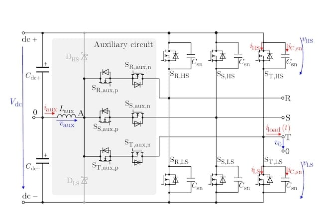
Figure 1. Circuit diagram of the three-phase ARCP with a single shared inductor. Image used courtesy of Bodo’s Power Systems [PDF]
Implementation of the S²I-ARCP Prototype
An 800 V, 15 kW prototype was built to validate this concept. It includes a control board, DC-link voltage measurement, three-phase current sensors, a main circuit board containing the B6-bridge and the DC-link at the bottom, and an auxiliary circuit board located at the top that incorporates a toroidal air-coil. To increase the snubber capacitance, NP0 MLCCs are connected in parallel to the output capacitance of the main switches.
Sanan 1200 V, 16 mΩ SiC MOSFETs serve as the main switches of the B6-bridge, while Sanan 1200 V, 20 mΩ SiC MOSFETs are used in the auxiliary circuit. The auxiliary switches can be rated for a lower current since current only briefly flows through the auxiliary circuit during commutation. A conventional sinusoidal modulation (other modulation methods are also applicable) generates the gate signals for the main switches. The detailed implementation of the operational strategy for the auxiliary switches, including collision avoidance, is provided in [2].
Figure 2 presents a photograph of the prototype, and Table 1 summarizes the key design parameters and components.
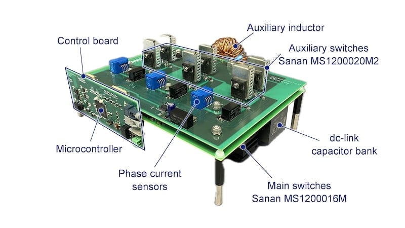
Figure 2. Experimental prototype of the three-phase S²I-ARCP. Image used courtesy of Bodo’s Power Systems [PDF]
Table 1. Main Design Parameters and Components of the Prototype.
| Parameter / Component | Value |
| DC-link voltage VDC | 800 V |
| Rated output power Pout | 15 kW |
| Switching frequency fsw | up to 40 kHz |
| Auxiliary inductor Laux | 5.5 μH (air coil) |
| Snubber capacitance Csn | 1 nF (NP0 MLCCs) |
| Dead-time Tdead | 185 ns |
| Main switches | SiC MOSFET Sanan MS1200016M |
| Auxiliary switches | SiC MOSFET Sanan MS1200020M2 |
| Cooling | Natural convection |
dv/dt Limitation and EMI Reduction
Power electronic designers can influence the converter’s EMI performance by selecting appropriate parameters and resonant components. The voltage profile can be shaped to comply with the application’s specific EMI requirements and dv/dt limits. Figure 3 shows the low-side (LS) to high-side (HS) transition.
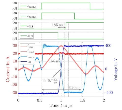
Figure 3. Switching transition waveforms. Image used courtesy of Bodo’s Power Systems [PDF]
Immediately before the switching event determined by the PWM modulation, both auxiliary switches are turned on at zero current (ZCS), which builds up a current in the auxiliary inductor that drives the resonant transition. Once the low-side switch turns off, Laux resonates with Csn, initiating the charging and discharging of the main switch output capacitances. The voltage across the high-side switch gradually swings down to zero in a slow, smooth, and sinusoidal manner until the conduction condition of the antiparallel diode is met. As soon as the high-side transistor’s antiparallel diode conducts, the HS transistor can be turned on at zero voltage (ZVS), significantly reducing switching losses.
The choice of resonant parameters (Laux and Csn) determines the commutation time, allowing for precise tuning of the maximum dv/ dt without sacrificing efficiency. The maximum dv/dt for this design is limited to just 6.7 kV/μs, which already meets most common industry requirements.
Efficiency and Power Losses
Figure 4 shows the inverter’s measured efficiency plotted against the output power, indicating values that exceed 99.6% across a wide load range - including part-load conditions, where switching losses usually dominate total losses. This level of efficiency allows for the omission of forced air/water cooling within that power range. Further studies [3] have demonstrated a total loss reduction of about 50% compared to a conventional hard-switched B6-bridge, along with the ability to significantly increase the switching frequency under identical cooling conditions.

Figure 4. Efficiency and total power losses for different loads. Image used courtesy of Bodo’s Power Systems [PDF]
By raising the switching frequency, the waveform quality of output voltage and current improves, which in turn reduces harmonic losses in a motor powered by the inverter and allows for a smaller capacitor size in the DC-link.
In soft-switching mode with SiC MOSFETs, switching losses can be decreased by up to 90% [3]. The remaining switching losses primarily occur during turn-off, mainly influenced by how quickly the MOS channel closes before the drain-source voltage rises (the V–I overlap). The speed of this turn-off transition depends on the transistor parameters and gate driver characteristics.
Why Should You Choose Sanan Semiconductor?
Sanan’s transistor portfolio is characterized by its exceptionally low internal gate resistance Rg,int - down to 0.9 Ω, and carefully optimized input and output capacitances Ciss/Coss. This synergy facilitates ultra-fast channel closure and a gentle voltage rise, minimizing the crucial V–I overlap during turn-off. The result is remarkably low switching losses in ZVS operation, providing unmatched efficiency and performance not only in hard-switched but also in soft-switched applications.
What are the Target Applications?
An interesting application for this topology would be the automotive traction inverter. Many automotive manufacturers already employ wide-bandgap semiconductors in their EV drive inverters. However, they often cannot fully utilize their high switching speeds due to system (e.g., motor winding) limitations, resulting in higher power losses and increased cooling requirements. Thanks to soft switching, this topology can decouple switching losses from dv/ dt slew rates, thereby reaching up to 90% lower switching losses under the same switching slew-rate conditions, enabling higher efficiencies and consequently lower size and volumes.
References
[1] R. W. de Doncker and J. P. Lyons, “The auxiliary resonant commutated pole converter,” in Proc. IEEE Int. Conf. Ind. Appl. Soc., Seattle, WA, USA, 1990, pp. 1228–1235.
[2] T. Lehmeier, A. Amler, Y. Zhou, and M. März, “Three-Phase ARCP Inverter Using Soft-Switching With a Single Shared Inductor,” IEEE Trans. Power Electron., vol. 39, no. 2, pp. 2505–2521, 2024.
[3] T. Lehmeier, A. Amler, Y. Zhou, and M. März, “Comparative Experimental Evaluation of a Three-Phase ARCP Inverter With a Single Shared Inductor Using SiC MOSFETs and Si IGBTs,” in Proc. IEEE Appl. Power Electron. Conf. Expo., Long Beach, CA, USA, 2024, pp. 547–554.
This article originally appeared in Bodo’s Power Systems [PDF] magazine and is co-authored by Thomas Lehmeier, Yan Zhou, Institute of Power Electronics, Friedrich-Alexander University of Erlangen-Nuremberg, and Ajay Poonjal Pai, Head of WBG Semiconductor Innovation, Munich, Sanan Semiconductor