Facebook
 Google
 GitHub
 Linkedin
SiC Wafer & Epitaxy Advances Enable Affordable Power Semiconductors
Improvements in SiC wafering and epitaxy manufacturing challenges are delivering affordable, high-efficiency power semiconductors.
This article is published by EEPower as part of an exclusive digital content partnership with Bodo’s Power Systems.
From renewable energy to electric mobility, silicon carbide (SiC) power semiconductors have become critical to pursuing sustainability through electrification. While the technology delivers a valuable efficiency advantage over silicon alternatives, SiC components remain relatively expensive due to manufacturing challenges. Overcoming these challenges holds the key to producing commercially viable components.
Growing SiC Crystals
Silicon carbide has a complex crystal structure with many different polytypes. It displays extreme hardness—two properties unsuited for fabricating precision electronic components with sub-micron feature sizes. While silicon ingots for wafer production can be produced routinely with close-to-perfect results, a SiC ingot, or boule, typically contains several types of defects resulting from imperfect growth.
Figure 1 shows the results of defective site analysis on a wafer of suitable quality for high-yield diode production.
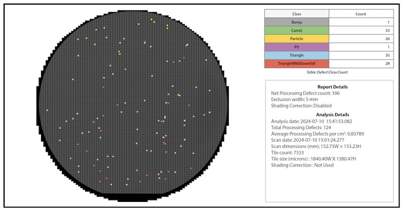
Figure 1. Defective site analysis of SiC wafer. Image used courtesy of Bodo’s Power Systems [PDF]
Among the most severe defects, basal plane dislocations (BPD) caused by misalignment of atoms can introduce strains that affect the overall integrity of the crystal lattice. On the other hand, defects such as screw dislocations (SD) form around an axis and can produce visible defects in the surface after epitaxy. Improving control over crystal-growth conditions, as well as applying post-growth treatments, can help to mitigate SD.
Carrot defects, conical or carrot-shaped inclusions in the SiC crystal, happen when screw dislocations intersect the surface of the crystal during growth, providing a channel for impurities to be incorporated into the crystal, causing carrot-shaped inclusions. There can also be hollow core dislocations, referred to as micropipes. Other potential causes of defects include irregular crystal stacking, missing atoms, extra atoms, and grain boundaries that can extend through the crystal lattice.
Wafering and Epitaxy Challenges
After the boule is grown, wafers are cut by sawing with diamond-encrusted wire saws and then ground and polished. These processes are time-consuming and expensive due to SiC’s extreme hardness, yet some defects inevitably remain in and below the substrate surface. When epitaxy is applied, these imperfections can impede layer growth, leading to step bunching, effectively slowing the formation of steps and causing interference and unwanted changes in the step height. Imperfections below the crystal surface affect device parameters such as the body diode characteristics and the interface quality with gate oxide.
In addition, local site flatness is much more difficult to achieve after grinding and polishing than ordinary silicon. However, a flat surface is critical for device fabrication to permit proper focusing of the lithography equipment and thus achieve accurate device dimensions, directly affecting the electrical parameters.
The stepper tries to focus on the center of each site. Because the depth of field of the lithographic equipment is relatively shallow, wafer shape variation means the image can be less sharply focused in some places. Subsequently, the reactor causes variations in epitaxial doping and thickness, resulting in a spread of device parameters. The breakdown voltage (BVDSS) of SiC MOSFETs is known to be particularly strongly affected (Figure 2). Severe defects at some sites on any given wafer may produce some dies that cannot function at all.

Figure 2. Measured BVDSS of MOSFETs fabricated at different sites across the wafer surface, showing radial variation due to epitaxial doping and thickness. Image used courtesy of Bodo’s Power Systems [PDF]
Defining Wafer Quality
The extent of imperfections in a wafer significantly affects the number of good dies the wafer will yield. More imperfections imply a lower yield that effectively drives up the per-unit component price. On the other hand, setting a high specification can raise the price of bare wafers.
When arranging the supply of SiC epiwafers, chip makers must specify the acceptable level of imperfections. The industry has had to learn how to establish workable specifications, enabling suppliers to deliver suitable quality cost-effectively while allowing device manufacturers to produce enough functional dies to remain commercially viable.
Epiwafer suppliers provide a certificate of analysis (CofA) that confirms conformance with the agreed specification. As understanding of the issues has grown, device manufacturers have requested epiwafer suppliers to provide more information in the CofA.
Early in SiC’s history, suppliers and device makers focused on only a few wafer parameters. Historically, for example, only the total count of defects on the wafer surface has been monitored. It is now common for the CofA to specify the percentage of sites that must be defect-free, with specific limits on defects of serious concern, such as BPD. The percentage of sites that have zero BPD defects is most important in wafers intended for MOSFET production.
Surface flatness, also, was typically stated for the entire wafer. Experience has shown that device manufacturers need assurances about flatness in more localized areas across the wafer surface. Accordingly, local site flatness has become a typically requested parameter.
Figure 3 shows a sample of parameters from a typical SiC epiwafer CofA. In this list, local site flatness is expressed as the SBIR, or (S)ite (B)ackside (I)deal Focal Plane (R)ange. Considering the surface topology as a set of peaks and troughs above and below the center point of the site, SBIR is the sum of the highest peak height and the lowest trough depth. Although an SBIR value of 2µm has been considered adequate, 1.2µm is a more acceptable range to minimize flatness deviation as a cause of defects in fabricated devices.
Processes and Equipment
Increasing knowledge of the types of defects in epiwafers, their causes, and their effects on component quality and performance has driven improvements in the processes and equipment available for wafer production.
Table 1. Key parameters specified in the CoƒA.
|
Epitaxial Layer Characteristics |
||
|
Epi-Layer1 (buffer) thickness |
1 |
μm |
|
Epi-Layer1 (buffer) doping concentration |
1.00 E18 |
At/cm3 |
|
Epi-Layer2 (drift) thickness |
14.5 |
μm |
|
Epi-Layer2 doping concentration |
6.0 E15 |
At/cm3 |
|
Post-epi Characteristics |
||
|
Warp, epi-wafer |
≤ 50 |
μm |
|
Bow, epi-wafer |
± 40 |
μm |
|
Total thickness variation (TTV), epi-wafer |
≤ 10 |
μm |
|
Epi-wafer Site Flatness; SBIR (LTV) MAX |
≤ 5 |
μm |
|
Epi-wafer Site Flatness; SBIR (LTV) |
≤ 2 |
μm |
|
Surface roughness |
< 0.5 |
nm |
|
Front Surface visual inspection requirements |
||
|
Scratches-cumulative |
≤ 150 |
mm |
|
Surface Defects Density |
< 0.5 (Typical 0.1) |
cm3 |
|
Defect Free Area (2 mm□) |
> 93 |
% |
|
BPD Density |
< 0.5 (Typical 0.1) |
cm3 |
|
BPD Free Area (2mm□) |
> 90 |
% |
SiC’s extreme hardness presents challenges from the earliest stages of wafering. Cutting discs or diamond-encrusted wire saws used to cut wafers from the boule face a high risk of breakage. Laser cutting allows more substrates to be wafered from the expensive boule and will likely be preferred shortly. Also, laser dicing can narrow the wasted “street” between adjacent dies and increase the die per wafer.
In addition, work is ongoing to minimize so-called edge exclusion and allow processes to be applied closer to the wafer edge. Better data about the material characteristics within 4-6 mm of the wafer edge can help to increase utilization of this area to produce more usable dies and lower the per-unit device cost.
Commercialization is also driving improvements in reactor design. Multi-wafer reactors become more economical as volume demand rises. On the other hand, processing a single wafer provides greater flexibility to perfect the setup. In addition, advancements in photolithographic motion control permit smaller step sizes that minimize and reduce instances of defects. The typical step size now is about 25% of the size in previous equipment generations.
Moreover, the depth of field is typically greater, allowing extra tolerance for surface flatness. Sites with larger SBIR can now yield devices with parameters that are within the acceptable range. Improvements that optimize the dopant vapor flow and wafer movement in the reactor also minimize the differences in device properties produced at different sites on the wafer by ensuring more uniform epitaxial doping and thickness.
In addition, best practices are adapting, such as regular reactor cleaning. As particles accumulate on the reactor’s internal components and mechanisms, removing these prevents downfall that can otherwise produce faults of various shapes and sizes in the wafer surface
SiC vs. Silicon
SiC is a far more challenging substrate than silicon at every stage of component manufacture, from ingot or boule production through wafering, epitaxy, lithography, and dicing. Understanding and overcoming these challenges has defined the technology’s journey from research to commercial availability. The technical justifications for adopting SiC in high-efficiency converters and drives are clear. The economic argument is becoming more persuasive with each improvement in production processes, equipment, and practice.
This article originally appeared in Bodo’s Power Systems [PDF] magazine and is co-authored by Tony Witt, Device Scientist, and Timothy Han, President, SemiQ.