Facebook
 Google
 GitHub
 Linkedin
Formic Acid Soldering: Enabling the Next Generation of Power Devices—Part 2
In part 2, we focus on application considerations and take a deeper look at case studies for prevailing solder material alternatives, including solder preforms and emerging solder paste technology.
This article is published by EEPower as part of an exclusive digital content partnership with Bodo’s Power Systems.
What are the advantages that formic acid soldering can offer for assembling power devices in terms of performance and cost-of-ownership? Having described the basics of this process in Part 1, this Part 2 of the story will focus on application considerations and take a deeper look at case studies for prevailing solder material alternatives, including solder preforms and emerging solder paste technology.
The targeted mission profile (environmental, electrical, and thermal operating conditions) and reliability expectations are key considerations in packaging design. While engineers seek to squeeze out as much efficiency as possible by pushing the performance boundaries in devices, cost is still equally important to enable the scale-up necessary for electrification in the automotive, energy infrastructure, and industrial sectors.
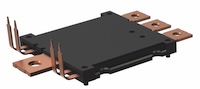
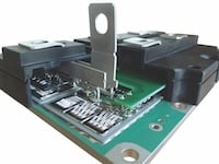
| Discrete | Molded Package | Baseplate Module | Dual-Side Cooling |
 |
 |
 |
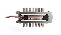 |
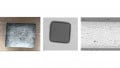
Figure 1. Common Power Device Form Factor Types. Image used courtesy of Bodo’s Power Systems [PDF]
There are several device form factor types that exist in the market, for example: discrete, molded package, baseplate, and dual-sided cooling. As such, unique characteristics exist for each type. However, the general construction or stack-up of these devices is common, and the performance and cost factors influence material selection for packaging, regardless of the device type.
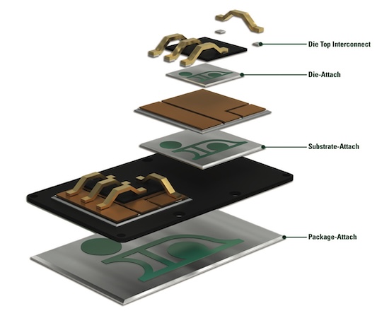
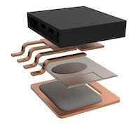
Figure 2. Typical Power Device Packaging Construction Stack-up. Image used courtesy of Bodo’s Power Systems [PDF]
Each interface—die top interconnect, die-attach, substrate-attach, package-attach—imposes distinct constraints on functional performance due to mechanical properties, thermal dissipation, and CTE mismatch. The corresponding metallization choices also have a direct influence over the wettability of the soldering material and the configuration parameters in the formic acid/vacuum reflow profile that are required for success.
For example, nickel finishes generally have a narrower soldering process window compared to copper or silver/gold-plated and may require extended formic acid soak time to remove oxides for effective solder wettability. Table 1 provides a summary of common packaging materials used in device stack-ups and constraints that must be considered in selecting the soldering alloy and reflow parameters.
Soldering Alloys
With regards to soldering alloy alternatives, it is worth noting that no single solution exists that will universally satisfy all mission profiles and packaging constraints. Therefore, trade-offs in both processability and performance must be considered by Design Engineers during selection:
- Metallization Compatibility, which affects wettability, reflow profile configuration parameters, and process window for formic acid soldering
- Minimizing Voiding, to achieve consistent thermal performance
- Process Temperature, which may influence sensitive materials in the device packaging, such as encapsulation, or affect reliability in multiple reflow stages
- Reliability Performance, considering the operating temperature and mission profile
- Environmental Sustainability, to reduce the use of lead in manufacturing (Pb-free)
Figure 3 lists commonly used alloys for power device soldering with formic acid:
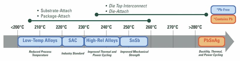
Figure 3. Common Solder Alloys used in Power Electronics Applications. Image used courtesy of Bodo’s Power Systems [PDF]
Table 1. Typical Power Device Packaging Construction Stack-up
| Packaging Component | Common Materials | Constraints | |
| Die Top Interconnect | Clip/Lead Frame | Bare Cu | Bondline Thickness |
| Die Top Metallization | Ti-NiV-(Au or Ag) or Ni-Pd-(Au/Ag) | CTE Mismatch | |
| Die-Attach | Semiconductor Die | Si, SiC, GaN | Junction Temperature |
| Die Bottom Metallization | Ti-NiV-(Au/Ag) or Ni-Pd-(Au/Ag) | Bondline Thickness | |
| Substrate-Attach | Ceramic | Al2O3, ZTA, Si3N4, AlN | Strength, Reliability |
| Substrate Metallization | DBC, AMB; Cu, ENIG, Ag-plated | Warpage | |
| Baseplate | Cu, AlSiC Aluminum Graphite (emerging) | Thermal Conductivity, Warpage, Thermal Mass | |
| Baseplate Metallization | Ni-plated | Solder Wettability | |
| Package-Attach | Heat-Sink/Cooler | Cu, Al | Thermal Conductivity, CTE Mismatch |
| Metallization | Ni-plated, Ag-plated Selective Cu (emerging) | Warpage, Solder Wettability |
Table 2. Common Failure Modes in Formic Acid Soldering with Preforms and Associated Actions for Improvement. Image used courtesy of Bodo’s Power Systems [PDF]
 |
Non-wetting, delamination due to excess surface oxidation. |
Increase formic acid temperature (180-250 °C) Increase formic acid soak time Verify formic acid flow rate, concentration |
|
|
Preform discoloration due
Corresponding non-wetting |
Preform manufacturing is not optimized for formic acid reflow
Increase formic acid soak time |
 |
Organic contamination on the preform surface increases localized voiding |
Preform manufacturing is not optimized for formic acid reflow Excess manual handling prior to assembly |
 |
Marginal voiding caused by Packaging weaknesses |
Preform packaging not optimized to maintain shelf life |
Solder Preform Applications
Solder preforms are custom-sized, solid, fabricated parts consisting of a given solder alloy, and can be produced to precise dimensions to closely match the targeted geometry in the device stack-up. For formic acid soldering applications, solder preforms are purely metal and contain no flux—this makes preforms the clear choice for larger area soldering, including substrate- and package-attach, where voiding and thermal performance are factors. Further, the engineering customization available with solder preforms allows for the precise tuning of solder volume that is consistent over mass production.
Figure 4. Solder Preform Configuration. Image used courtesy of Bodo’s Power Systems [PDF]
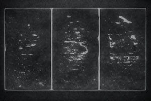
While formic acid soldering with preforms offers performance, quality, and scalability advantages, vulnerability to material contamination and excess oxidation narrows the process window for success and poses challenges to solder preform manufacturing. To illustrate these challenges, this story will dig further into the substrate-attach application. In this case, the relatively larger area of the soldering interface means more surface area to reduce oxidation and a greater risk for contamination due to manufacturing methods. Table 2 shows common failure modes in formic acid soldering with preforms and associated actions for improvement.
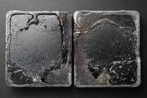
Indium Corporation has developed specialized solder preforms designed specifically for use in formic acid reflow to minimize surface oxidation and growth over time, prevent any possible contamination, and maximize shelf life. This approach has been proven to deliver really low voiding and maintain a stable shelf life for robust wetting over time, as shown in Figures 5 and 6.
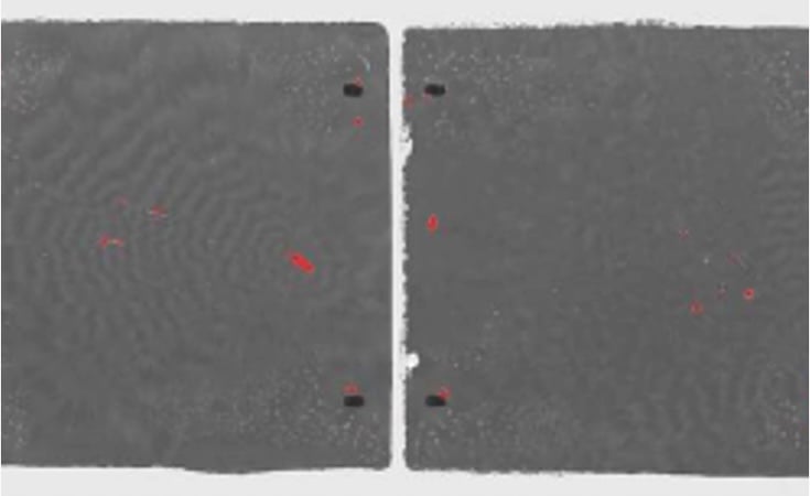
Figure 5. Specialized SnSb Preform results in <1 % Voiding in Substrate-Attach with Formic Acid/Vacuum Soldering. Image used courtesy of Bodo’s Power Systems [PDF]
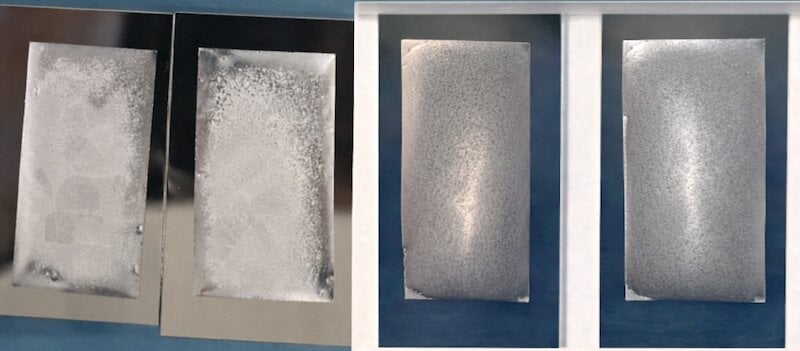
Figure 6. Robust Wetting of SnSb Preforms on Ni Baseplate: Month 1 (Left) Compared to >12 Months (Right). Image used courtesy of Bodo’s Power Systems [PDF]
Emerging Fluxless Solder Paste Technology
Conventional solder pastes leverage a flux vehicle, consisting of rosins, resins, and activators, to both reduce oxides during reflow and maintain the necessary rheology to apply the solder through printing or dispensing. In a formic acid reflow environment where flux is not required, these components in conventional solder paste produce residues that can contaminate the material integrity and often require post-process cleaning. Ongoing innovations in fluxless solder paste have resulted in new technologies that leverage a complex solvent system as a binder with thixotropic agents that enable dispensing and printing, while leaving virtually no residue after reflow.
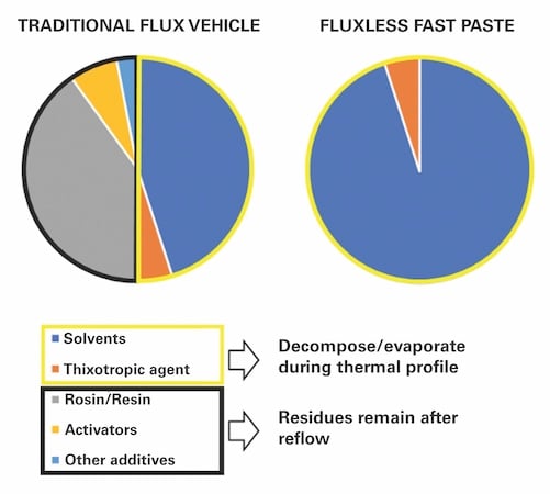
Figure 7. Comparison of Flux and Fluxless Binder. Image used courtesy of Bodo’s Power Systems [PDF]
The evaporation of the fluxless paste binder components during reflow is a critical design characteristic to promote solid wettability and eliminate residue in formic acid reflow. Thermogravimetric analysis (TGA) is a technique used to measure the change in mass of a material as a function of temperature and/or time under a controlled atmosphere. The comparison bin figure 8 demonstrates the absence of residues with fluxless paste after reflow compared to conventional solder pastes.
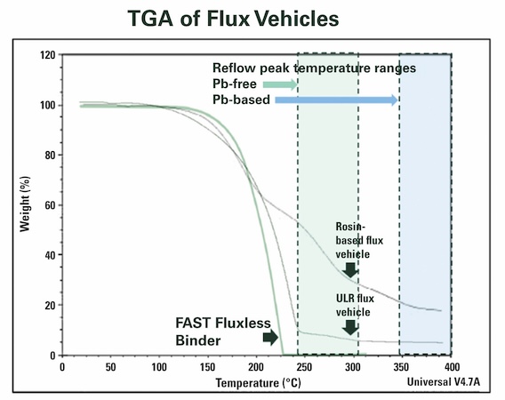
Figure 8. TGA of Fluxless Solder Paste Compared to Conventional Solder Paste. Image used courtesy of Bodo’s Power Systems [PDF]
This technology offers a compelling solution for die and component-level soldering in the power device stack-up to reduce equipment footprint and improve voiding for overall performance gains. A case study was performed to characterize solder wettability, voiding, and delamination for die-attach (10 mm x 10 mm, 5 mm x 5 mm) and component-attach, i.e., thermistors, using open samples, as well as die-capped samples inspected via acoustic microscopy. The results below indicate solid wetting, consistent edge quality, and ultra-low voiding for the fluxless paste.
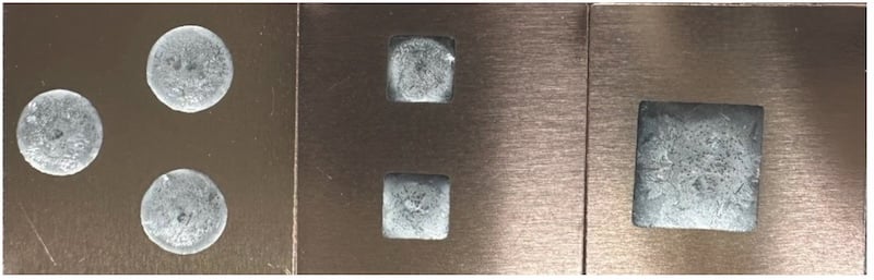
Figure 9. Reflow Results for High-Pb Fluxless Solder Paste – Component-Attach. Image used courtesy of Bodo’s Power Systems [PDF]
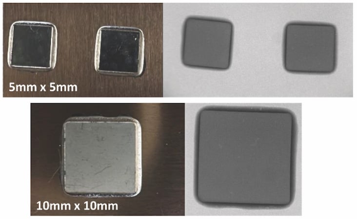
Figure 10. Reflow Results for High-Pb Fluxless Solder Paste – Die-Attach. Image used courtesy of Bodo’s Power Systems [PDF]
Die shear, a commonly used technique to determine the quality of the die-attach process, was also carried out to compare the bond strength for fluxless solder paste with formic acid reflow vs. typical values expected from standard high-lead solder with a conventional reflow process. Die shear was carried out at time zero (post reflow) and after both 500 cycles and 1,000 cycles of thermal cycling between -65°C and 150°C.
Typical die shear values for high-lead solder are between 20 - 40MPa, depending on other factors such as surface finish or process conditions, and this was the case for the fluxless paste reflowed with formic acid. The average die shear strength at time zero was 31.7MPa, after 500 cycles, the average was 28MPa, and after 1,000 cycles, the average was 28.3MPa. This showed that the die shear strength for fluxless paste reflowed with formic acid was comparable to that of traditional solder paste with a conventional reflow for the same alloy system.
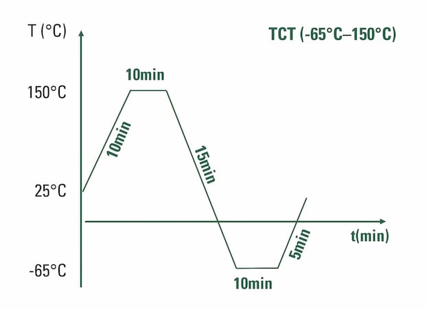
Figure 11. Thermal Cycling Profile. Image used courtesy of Bodo’s Power Systems [PDF]
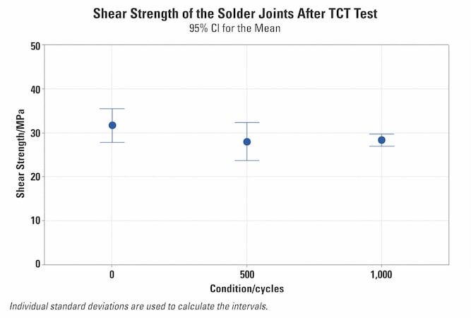
Figure 12. Die Shear Results. Image used courtesy of Bodo’s Power Systems [PDF]
Conclusion
Formic acid soldering has transitioned from a niche process to a mainstream solution, especially in power electronics manufacturing. It rests on three pillars:
- Material Cleanliness and Stack-up Design – metallization and surface oxide/contamination characteristics influence the process window
- Reflow Process Control – careful consideration of factors affecting formic acid fluxing activity, temperature, and vacuum
- Solder Material and Quality – specially developed materials for formic acid soldering maximize yields and enable increased device performance
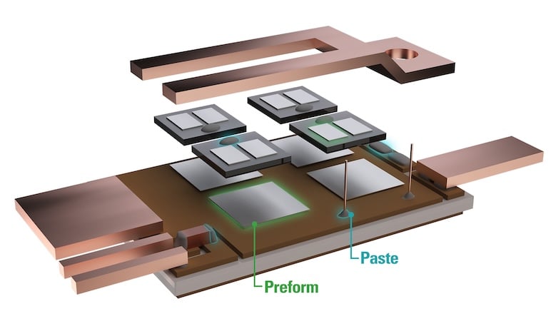
Figure 13. Future Power Device Architectures Can Leverage both Fluxless Solder Preforms and Paste. Image used courtesy of Bodo’s Power Systems [PDF]
With mature formic acid soldering processes, proven solder preform solutions, and emerging fluxless paste technology, engineers have more choices than ever to balance the performance and cost-of-ownership goals for future power device designs. With the progression of materials technologies, both solder preforms and fluxless paste can be incorporated into a single packaging design. This offers a completely fluxless solution for the entire device stack-up to achieve unprecedented flexibility and efficiency with formic acid reflow processes, enabling the Next Generation of Power Electronics devices.
This article originally appeared in Bodo’s Power Systems [PDF] magazine.