Facebook
 Google
 GitHub
 Linkedin
Renesas Unveils 650 V GaN FETs for Power Conversion
The GaN releases expand Renesas’ ecosystem-driven approach for the wide bandgap semiconductor.
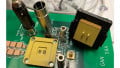
Renesas has introduced a family of 650 V GaN FETs focusing on high-efficiency, high-density power conversion for data center, industrial, and e-mobility applications. EEPower attended a briefing with Primit Parikh, Vice President of Renesas’ GaN Business Division, to learn more about the solutions firsthand.
Renesas’ 650 V GaN FETs. Image used courtesy of Renesas
The TP65H030G4P Family
The TP65H030G4P family marks the company’s first major product launch since acquiring GaN pioneer Transphorm in 2024, which combines Transphorm’s SuperGaN d-mode platform with Renesas’ packaging expertise and roadmap integration.
Parikh explained, “The GaN business division has come about via the acquisition of Transphorm... now all coming together to enable us what we call a GaN ecosystem—a product-based offering. By a GaN ecosystem, we mean gallium nitride devices, ICs, drivers, controllers, and solutions.”
These fourth-generation plus (Gen IV Plus) devices are built on a smaller 14% reduced die, offering a 30 mΩ RDS(on), and a 20% improvement in output-capacitance-product figure of merit compared to previous Gen IV devices.
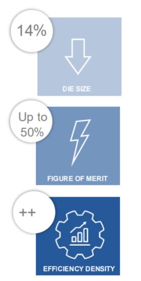
Improvements in the GaN generation from Renesas. Image used courtesy of Renesas
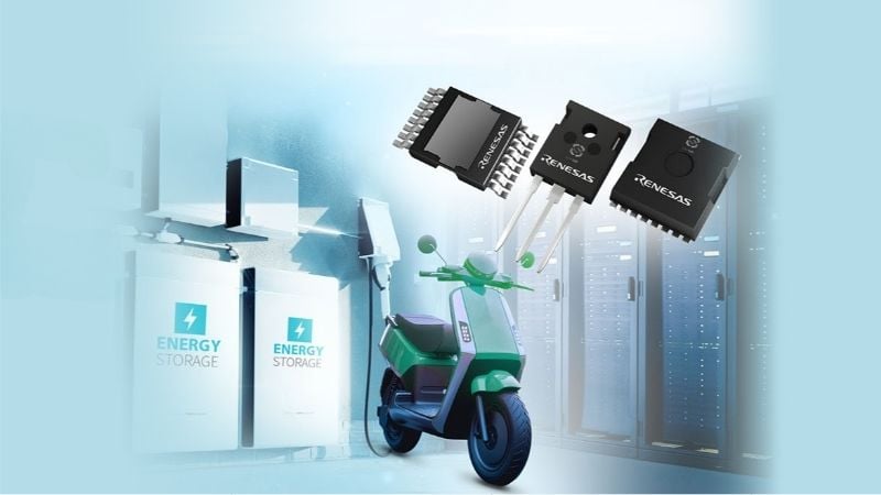
The GaN FETs, TP65H030G4PQS, TP65H030G4PWS, and TP65H030G4PRS, support power conversion from 1 kW to 10 kW and above and are intended for a variety of emerging 800 V HVDC topologies in AI server power supplies, totem-pole PFCs in fast EV chargers, UPS systems, and inverter designs for solar and energy storage systems.
d-Mode SuperGaN Design with Silicon-Compatible Drive
The Gen IV Plus platform utilizes a cascode configuration that combines a depletion-mode GaN HEMT with a low-voltage silicon MOSFET to create a normally off device. With this structure, Renesas eliminates the need for custom GaN gate drivers and allows easy integration into existing silicon-based gate driver circuits.
“Because of the cascode structure, our GaN FETs can be driven by standard silicon gate drivers,” Parikh explained. “You don’t need exotic or custom drivers, which reduces system complexity and cost.”
Renesas’ d-Mode GaN configuration. Image used courtesy of Renesas
The devices also achieve a 4 V threshold voltage for improved noise margin and gate control reliability, which Renesas claims is not possible with enhancement-mode GaN.
Additionally, switching characteristics are enhanced through reductions in gate charge, output capacitance, crossover loss, and dynamic RDS(on). By leveraging a smaller die, the architecture also lowers output capacitance, enables faster switching transitions, and reduces losses in high-frequency designs. The 14% smaller die also minimizes switching-related heat and contributes to lower system costs by reducing silicon area and passive component sizing.
Thermal Design Flexibility
To accommodate varying thermal and layout constraints, Renesas offers the Gen IV Plus devices in three packages: TO-247, TOLL, and TOLT. The TO-247 provides enhanced thermal capacity with through-hole mounting for high-power systems. TOLL offers a compact, bottom-side cooled surface-mount option for reduced PCB footprint. At the same time, TOLT introduces a top-side cooled surface-mount format that enables easier paralleling of devices and improved thermal performance in high-conduction-current designs.
The package portfolio allows designers to trade off between PCB density, heat sinking, and manufacturability.
Manufacturing Maturity and Deployment Scale
To date, Renesas reports over 20 million GaN units shipped and 300 billion hours of cumulative field operation. To support this demand, the company has vertically integrated its manufacturing chain, controlling epitaxy and wafer processing, and is scaling from 6-inch to 8-inch wafers to reduce the cost per ampere. Licensing and supply agreements are in place to accelerate this transition by 2027.
With an expanding portfolio that includes high- and low-power variants, reference platforms, and driver co-development, Renesas is truly consolidating the space with an ecosystem-led strategy that aims at system efficiency, integration, and ease of deployment.
Looking to the future, Parikh explained, “Especially now that the cost figure of merit of GaN is becoming very competitive, and manufacturing is also scaling to larger diameter wafers ... GaN is now ready for growth to support the major semiconductor industry megatrends.”