Facebook
 Google
 GitHub
 Linkedin
Using Low-Voltage GaN in ISOP Converters for AI Servers With 800 V Architecture
Over the past decade, AI workloads have relied on server architectures not designed for their rapidly growing power demands. Recently, the concept of “AI factories” has emerged, reframing data centers as productivity-driven systems optimized for high compute density.
This article is published by EEPower as part of an exclusive digital content partnership with Bodo’s Power Systems.
Article co-authored by Efficient Power Conversion's Michael de Rooij.
To maximize throughput within limited physical space, AI infrastructure has dramatically increased processor density, creating competition between computing hardware and power supplies for rack space. This challenge has led to the adoption of an 800 VDC power distribution architecture, which reduces losses, supports much higher power levels, and allows bulky power components to be moved out of IT racks into a separate power rack, as shown in Figure 1. As a result, rack power capacity can scale from roughly 200 kW to over 1 MW [1], significantly enhancing AI computing capability.
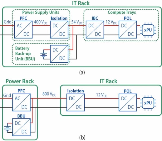
Figure 1. AI Server architectures: a) Traditional 54 V distribution bus, b) New 800 VDC distribution. Image used courtesy of Bodo’s Power Systems [PDF]
Under the new architecture, IT racks mainly contain compute trays powered directly from an 800 VDC bus. Although this shift introduces challenges related to voltage ratings and isolation, it also encourages new high-efficiency, high-power-density conversion topologies. Because multiple conversion stages exist between the grid and the xPUs - and not all require tight regulation - the isolation stage supplied by the regulated 800 VDC bus is a strong candidate for architectural innovation. Accordingly, this article focuses on the isolation stage and presents an Input-Series-Output-Parallel converter designed for AI server racks.
Input-Series-Output-Parallel (ISOP) Converters
Multilevel topologies, including ISOP architectures using LLC converters, are emerging as popular solutions for the isolation stage in AI servers [2-4]. An ISOP converter uses multiple isolated modules with series-connected inputs and parallel-connected outputs.
This offers a convenient approach to scale both input voltage and output current simultaneously. Specifically, for a converter using M modules with input voltage VIN and output power POUT, each only experiences VIN/M and processes POUT/M.
Although multilevel or multiphase converters typically raise concerns regarding voltage balancing and current sharing, LLC-based implementations can achieve both inherently through design, without dedicated control algorithms [5-6]. By selecting an appropriate magnetizing inductance-to-resonant inductance ratio (Lm/Lr), the converter gain becomes largely independent of frequency when operating at resonance, rendering a robust solution insensitive to component tolerances. Furthermore, the operation of the LLC converter at resonance also coincides with its most efficient operating mode. The tradeoff of this design choice is a reduced capability for output voltage regulation, which is why such solutions are typically implemented as fixed-ratio converters.
Compared to a conventional LLC converter, modular LLC-ISOP architecture offers reduced voltage stress in the primary side, simpler transformer design, lower output current ripple through interleaving, and improved thermal management [2]. This article expands on these benefits and presents details and experimental results for an 800 V to 12.5 V, 6 kW ISOP converter.
Low Voltage Stress in the Primary Enables Better Devices
To quantify some of these advantages, various semiconductor technologies are evaluated under a common set of assumptions. A 64:1 converter operating from 800 V to 12.5 V at 6 kW is considered, with a resonant frequency of 1 MHz and ZVS transition time limited to 5% of the switching period (tZVS = 50 ns). A half-bridge primary topology is assumed. These constraints fix the transformer design and current waveforms, enabling a consistent comparison across converter topologies and device technologies.
The analysis first determines the required magnetizing inductance to guarantee ZVS within the specified transition time. The primary rms current is then calculated [7], followed by conduction and gatedrive losses [8], which are combined to obtain the total primary-side semiconductor loss for a converter with M modules. Equations (1)–(6) summarize this methodology, where RL is the equivalent load per module and n is the number of primary turns (32 for a conventional LLC, 16 for 2-module ISOP, and 4 for 8-module ISOP).
\[L_{m}=\frac{n\cdot V_{OUT}\cdot t_{ZVS}}{8\cdot f\cdot Q_{OSS}}\,\,\,\,\,(1)\]
\[I_{P\,rms}=\frac{V_{OUT}}{8\cdot n\,\cdot R_{L}}\cdot\sqrt{\frac{2\cdot n^{4}\cdot R_{L}^{\,\,\,2}}{L_{m}^{\,\,\,\,2}\cdot f^{2}}+8\cdot\pi^{2}}\,\,\,\,\,(2)\]
\[R_{L}=M\cdot\frac{V^{\,\,\,\,\,\,\,\,\,\,\,2}_{OUT}}{P_{OUT}}\,\,\,\,\,(3)\]
\[P_{ON}=M\cdot R_{DS(on)}\cdot I_{P\,rms}^{\,\,\,\,\,\,\,\,\,\,\,\,\,\,\,2}\,\,\,\,\,(4)\]
\[P_{G}=M\cdot V_{drive}\cdot 2\cdot Q_{G}\cdot f\,\,\,\,\,(5)\]
\[P_{tot}=P_{ON}+P_{G}\,\,\,\,\,(6)\]
Table 1 compares primary-side devices for both conventional LLC and LLC-ISOP configurations. While single-module LLC implementations rely on 1.2 kV SiC devices, increasing the number of ISOP modules enables the use of lower-voltage SiC and GaN devices.
The results show that the 8-module ISOP configuration using 150 V GaN devices achieves the lowest total primary-side loss (Ptot). A similar trend is seen in board area. All evaluated devices use surface-mount packages compatible with top-side liquid cooling. The most compact solution again corresponding to the 8-module ISOP implementation using 150 V–rated GaN.
Table 1. Performance comparison of primary-side devices.
| Case | Topology | M | n | Primary FETs [Part Number] | Qty | RDS(on) (mΩ) | Qg (nC) | Vdrive (V) | Qoss (nC) | Ptot (W) | Area (mm2) |
| 1 | LLC | 1 | 32 | SiC 1.2 kV [IMCQ120R004M2H] | 2 | 3.7 | 348 | 18 | 898 | 15.9 | 630 |
| 2 | SiC 1.2 kV [IMCQ120R017M2H] | 2 | 17.1 | 91.1 | 18 | 196 | 8.6 | 630 | |||
| 3 | ISOP-LLC | 2 | 16 | SiC 650 V [IMDQ65R007M2H] | 4 | 6.7 | 179 | 18 | 337 | 17.8 | 600 |
| 4 | SiC 650 V [IMDQ65R015M2H] | 4 | 14.5 | 79 | 18 | 148 | 14.2 | 600 | |||
| 5 | GaN 650 V [IGLT65R025D2] | 4 | 25 | 41 | 3.7 | 82 | 14.8 | 600 | |||
| 6 | 3 | 4 | GaN 150 V [EPC2305] | 16 | 2.2 | 22 | 5 | 120 | 6.8 | 240 | |
| 7 | GaN 150 V [EPC2308] | 16 | 4.5 | 11.7 | 5 | 50 | 11.0 | 240 |
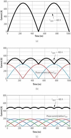
Figure 2. Rectified secondary-side current for a conventional LLC converter (a), an ISOP converter with 2 interleaved modules (b), and an ISOP converter with 4 interleaved modules (c). Image used courtesy of Bodo’s Power Systems [PDF]
Interleaving of PWM Signals for the Modules to Reduce Output Current Ripple
Analogous to multi-phase buck converters, the ISOP modules can be interleaved to reduce output current ripple, which in turn lowers the required output capacitance for a given voltage ripple. For the converter described earlier, a conventional LLC must handle a peak-to-peak current of ≈ 754 A with a ripple frequency of 2 MHz, while a 2-module ISOP experiences ≈ 156 A at 4 MHz, and a 4-module ISOP only ≈ 37 A at 8 MHz. This comparison is illustrated in Figure 2.
800 V to 12.5 V ISOP Converter Using 8 modules
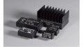
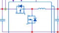
To demonstrate an 8-module ISOP converter, EPC developed and tested the 6 kW, 800 V to 12.5 V (64:1) fixed ratio converter shown in Figure 3. The design comprises 8 identical modules, each a 100 V to 12.5 V LLC converter rated at 750 W. Figure 4 shows a simplified diagram of the converter alongside the schematic of a single LLC module.
The primary side uses two EPC2305 GaN transistors in a half-bridge configuration. The EPC2305 is a 150 V-rated device with a typical RDS(on) = 2.2 mΩ, packaged in a 3 mm x 5 mm QFN. The secondary side uses two paralleled EPC2366 in a center-tap configuration. The EPC2366 is a 40 V-rated GaN device with a typical RDS(on) = 0.8 mΩ, in a 2.6 mm x 3.3 mm QFN package. Primary and secondary sides are magnetically coupled via a planar transformer with a 4:1:1 turns ratio. The transformer windings are integrated into a 14-layer PCB, and the core uses a standard ER geometry fabricated using Proterial ML95S material.
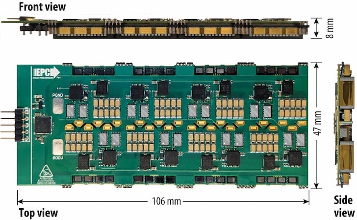
Figure 3. Top, front and side photos of the ISOP converter. Image used courtesy of Bodo’s Power Systems [PDF]
The complete converter, with an overall thickness of 8 mm, occupies less than 5000 mm² of board area, including controller and digital isolators with reinforced isolation. All the GaN devices are mounted on the top-side of the board to facilitate cooling, either via a heatsink or a water-cooled cold plate.
The converter was tested with an input voltage of 800 V and delivering output currents up to 500 A. Figure 4 presents the measured efficiency and power losses as a function of load current, showing a peak efficiency exceeding 98% and a full-load efficiency of 96.4%.
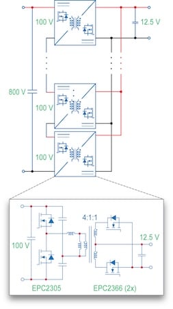
Figure 4. Block diagram of the ISOP converter and simplified schematic of the LLC modules. Image used courtesy of Bodo’s Power Systems [PDF]
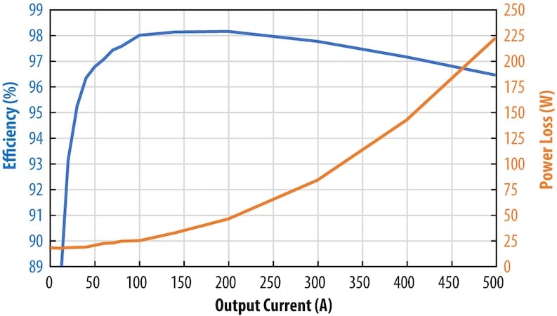
Figure 5. Efficiency and Power Loss curves for the ISOP converter delivering up to 500 A into a 12.5 V load from an 800 V input. Image used courtesy of Bodo’s Power Systems [PDF]
Conclusions
ISOP converters offer high-efficiency, high-power-density solutions for AI server racks by reducing primary-side voltage stress, lowering output current ripple, and simplifying transformer design. Experimental results for an 800 V to 12.5 V, 6 kW converter using an 8-module ISOP-LLC with 150 V-rated GaN transistors demonstrate peak efficiency above 98% and full-load efficiency of 96.4%. These results highlight the potential of ISOP architectures to meet the stringent efficiency, power density, and form-factor requirements of modern AI infrastructure.
References
[1] J. Huntington, M. Tu, “800 VDC Architecture for Next-Generation AI Infrastructure,” Nvidia, October 2025.
[2] A. Pozo, S. Colino, “Case Study: A Low Cost and Low Profile 800 VDC to 12.5 V DC-DC Converter Using Low Voltage GaN in an ISOP Topology,” Efficient Power Conversion article on EEPower.
[3] “Redefining Data Center Power: GaN and SiC Technologies for Next-Gen 800 VDC Infrastructure,” Navitas Semiconductor.
[4] G. Deboy, “Power Conversion Solutions for future Server Boards operating directly from HV DC,” 2025 OCP Global Summit, San Jose, California, 2025.
[5] A. Pozo and M. A. de Rooij, “5.5 kW Isolated 400 V to 50 V DC-DC Converter for Server Power Supplies,” PCIM Conference 2025; International Exhibition and Conference for Power Electronics, Intelligent Motion, Renewable Energy and Energy Management, Nürnberg, Germany, 2025.
[6] Q. Ma, Q. Huang, and A. Q. Huang, “Zero-Voltage Switching and Natural Voltage Balancing of a 3 kW 1 MHz Input-Series-Output-Parallel GaN LLC Converter,” in IEEE Open Journal of Power Electronics, vol. 5, pp. 1119-1128, 2024.
[7] Bing Lu, Wenduo Liu, Yan Liang, F. C. Lee, and J. D. van Wyk, “Optimal design methodology for LLC resonant converter,” Twenty-First Annual IEEE Applied Power Electronics Conference and Exposition, 2006. APEC ‘06, Dallas, TX, USA, 2006.
[8] A. Lidow, M. De Rooij, J. Glaser, A. Pozo, S. Zhang, M. Palma, D. Reusch, and J. Strydom, “GaN Transistors for Efficient Power Conversion,” 4th ed. John Wiley & Sons, 2025. ISBN: 978- 1394286959.
This article originally appeared in Bodo’s Power Systems [PDF] magazine and is co-authored by Alejandro Pozo and Michael de Rooij, Efficient Power Conversion
Related Content