Facebook
 Google
 GitHub
 Linkedin
Overcoming Challenges to Characterize 100V GaN Power FETs
The applications for 100V (and less) GaN FETs are numerous - from reducing distortion in Class-D audio amplifiers to improving efficiency in synchronous rectifiers and motor drives.
100 V GaN FETs are popular in 48 V automotive and server applications, as well as USB-C, lidar, and LED lighting. However, the small size and minimal packaging parasitics create multiple challenges to dynamically characterize these power devices. This article reviews the challenges GaN semiconductors manufacturers face to characterize these devices, as well as some new technologies that help address these challenges.
In recent years, widebandgap (WBG) devices have significantly progressed in replacing Si-based power MOSFETs and IGBTs in many power-related applications. Their fundamental characteristics enable significant improvements in key areas for power applications. When comparing GaN to Si, it is well known that GaN’s higher bandgap, higher electron mobility and larger electric field potential enable important attributes, such as lower losses (i.e., higher efficiency), faster switching (e.g., > MHz) and a significantly reduced size (i.e., higher power density). However, WBG devices have a much shorter history of use in a variety of power applications compared to Si, especially ‘high uptime’ applications like automotive.
JEDEC® formed the JC-70 Committee in 2017 to develop needed new reliability, characterization, test methods, and datasheet enhancements to appropriately characterize GaN and SiC WBG power devices. The existing Si-based standards were not sufficient to enable designers to determine the most appropriate WBG devices for their application. For example Rds(on), the main parameter characterizing conduction losses, is a dynamic phenomenon in GaN, based on the charge being trapped in the transistor structure (current collapse). JEP-173 was JC-70’s first publication (issued in January 2019) to provide a standard for ‘Dynamic ON-Resistance Test Method Guidelines for GaN HEMT based Power Conversion Devices’.
Examples of 100V GaN FET Applications
One application of the initial Class D audio amplifiers was automobile sound systems. The amplifier’s lower power dissipation and superior efficiency( > 90%) compared to Class A amplifiers enabled ‘limited power’ automobiles the ability to have multiple speakers and more sound (> 100W). However, the tradeoff for less power consumption was higher total harmonic distortion (THD) created by slower switching power Si MOSFETs. GaN FETs with significantly faster switching speeds (up to 10x) and no reverse recovery charge provide superior linear response and significantly reduced THD. In addition to automotive applications, recently you’ve probably noticed the boom in portable speakers. In addition to advances in battery technology, this application is enabled by efficient, compact Class D audio amplifiers designed with GaN FETs. Good audio quality is provided because of the lower distortion attributes of GaN, while the ability to run for extended times on batteries is possible because of GaN’s high efficiency. There are many other portable consumer devices that can leverage the same attributes as portable speakers.
Automotive systems are moving toward higher voltage operation (e.g., 48V) as more electrical power needs develop for autonomous driving, including radar, cameras, ultrasonic sensors, and lidar. These functions require uninterrupted, highly reliable power. As the 48V bus emerges as one of the new higher voltage power systems, efficiency is again the key with a limited power source (i.e. car battery). GaN technology enables better power density than Si, minimizing additional weight, size, and thermal management. GaN’s higher frequency switching, and increased efficiency also reduces necessary passive component size (e.g., inductors) further minimizing the size of the power converter design. DC-DC converters (12V – 48V) made from these GaN FETs, enable the standard 12V power bus to supply power for these emerging automotive system requirements.
Motor drives (e.g. stepper motors, drones, etc.) is yet another large application for 100V and less GaN devices. Low losses often remove the need for heat sinks. GaN enables higher frequency PWM signals and significantly reduces switching losses. Higher frequency switching reduces/eliminates switch node oscillations, often requiring snubber circuits in Si-based designs.
The are many evolving applications primed to take advantage of GaN’s superior performance compared to Silicon. But the challenges to characterizing these devices follow the themes described above: small size (power density) and higher efficiency.
Challenges Characterizing 100V GaN Power Devices
The first major challenge is the package size. Many of the 100V (and less) GaN FET packages are ball grid arrays (BGA) ranging from a few mm in the X and Y dimensions to sub mm in the X and Y dimensions. These packages have a 2x2 matrix of solder balls to a 5 x 15 matrix of solder balls. Figure 1 shows an example of an EPC2045, 100 V, 16 A GaN eHEMT device with a specified RDS(on) of 7 mΩ.

Figure 1. EPC 2045A dimensions (source: EPC2045A Datasheet, 2021.). Image used courtesy of Bodo’s Power Systems [PDF]
BGAs like the one used for the EPC 2045A, add little additional parasitic to the die of the GaN devices, making them ideal to take advantage of the superior performance of the high-speed switching applications. Why is minimizing package parasitics important? Primarily for repeatable and reliable dynamic performance of the device. Higher parasitics lead to more ringing and potential instability of the switching power FET. Figure 2 shows a standard DPT test configuration/model with fixture parasitics and the package/ device parasitics. (NOTE: This picture was taken from Keysight’s article in the April 2020 edition of Bodo’s Power Systems, entitled, “Overcoming Challenges Characterizing High Speed Power Semiconductors”. See this article for more details regarding the effects of parasitics in DPT waveforms.).

Figure 2. Primary parasitics needing consideration during DPT fixture design. Image used courtesy of Bodo’s Power Systems [PDF]
Because the parasitics of the GaN HEMT and BGA package are so low (e.g. typically < 1 nH, this GaN FET can switch at very high frequencies (e.g. 1MHz). To enable the high frequency switching energy to be accurately characterized, the DPT fixture must also have low parasitics, especially in the power loop and gate loop. These loops should be designed with low single-digit nH inductance (e.g. 3 nH or less) in mind to minimize the effect of the DPT fixture. Ideally, the fixture parasitics are less than the device/package parasitics, which is extremely difficult to accomplish for these small GaN FETS.
Additionally, creating a repeatable and reliable DUT connection method to enable a statistically valid sample size (e.g. >10) of GaN FETs to be tested is very challenging. The ideal situation is to solder each device on the fixture’s PCA. However, repeated soldering and unsoldering can easily damage a PCA. The mechanical tolerances needed to repeatably contact a solder ball require sub mm placement accuracy in both X and Y dimensions (see Figure 1: dimensions c, d, and e).
As mentioned above, the other major challenge is repeatably characterizing the GaN FET’s efficiency. There are three dynamic parameters that are the main factors that influence efficiency: 1) conduction loss, 2) switching loss, and to a lesser extent 3) drive loss.
1. Conduction Loss (Rds(on)) – As mentioned above, Rds(on) is a dynamic measurement for GaN HEMT devices. The JEP-173 provides guidelines for measuring and extracting this parameter. What is needed to determine this parameter repeatably and reliably is a very low parasitic DPT fixture providing clean Vds and Id switching waveforms. In addition, a fast clamp circuit is needed to settle quickly, enabling a measurement of the clamped Vds and Id 50-500ns after the switching event. These techniques will provide the best Rds(on) measurement to compare against stress voltages and timeframes to characterize the current collapse in the GaN FET structure.
2. Switching Loss (i.e., td(on), tr, E(on), td(off), tf , E(off)) – These parameters are specified in the IEC 60747-8 standard and are typically specified in Power FET datasheets. The ability to measure and extract these parameters repeatably and reliably is highly dependent on the fixture design and minimization of parasitics. Test conditions typically include Vds, Id, Vgs, sometimes the Lload, but almost always the gate resistor Rg. Rg is one of the main controls of the gate drive speed and, ultimately, how hard the device is turned on. Most ideally, Rg is a small value, allowing for a fast-switching transition. However, if the DPT fixture design is not optimized and has unwanted parasitics, then a larger Rg is needed to slow down the switching waveforms to minimize ringing.
3. Drive Loss (i.e., Qg) – Drive loss is typically the smallest of the losses. Repeatable and reliable measurement and calculation of gate charge (Qg), requires clean switching waveforms, specifically Vgs and Ig. Minimal gate loop parasitics are critical for clean waveforms.
Repeatable and Reliable Dynamic Characterization of 100V Gan FET
The key to obtaining repeatable and reliable dynamic characterization of small GaN FETs is in attention to detail of the DPT fixture design. An EPC 2045A described in Figure 1 was used as the target DUT.
Design Modifications to Keysight’s Customized GaN Solution
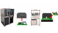
In the article “GaN Power Semiconductor Device Dynamic Characterization” in Bodo’s Power System October 2020 edition, Keysight’s solderless DUT connection technology (Figure 3 & Figure 9) for the PD1500A Dynamic Power Analyzer/Double Pulse Tester was presented. However, this connection technology had not been tested with as small a device as the EPC 2045A (1.5 mm x 2.5 mm), requiring repeatable connections to the gate, a single 44.5 µm2 round solder ball target. Fixturing and registration of these small GaN FETs are critical. A customized board for this device was developed to determine if Keysight’s solderless contact technology would provide repeatable results for this challenging device (see Figure 3).

Image used courtesy of Bodo’s Power Systems [PDF]

Image used courtesy of Bodo’s Power Systems [PDF]
Figure 3. Customized GaN board for EPC 2045A.
After a couple of design iterations to the device holder, including spring tension on the top plate and alignment holes for the base plate part registration, we successfully tested multiple sets of parts with this design.
To further minimize loop areas for the gate loop and power loop, a multi-layer PCB was leveraged, enabling trace routing within different layers to minimize the loop areas. The gate drivers and replaceable Rg daughter boards were placed on the back side of the PCB, further reducing loop areas.
Finally, a simplification of Keysight’s patent pending current sensor technology, also mentioned in the October 2020 article, allowed the shunt to be placed closer to the DUT, reducing power loop area, while further minimizing the insertion inductance of the sensor. Together, these modifications to Keysight’s existing customized GaN solution enabled industry-leading results for devices like the EPC 2045A.
Conduction Loss (Rds(on))Results
The test system setup to measure dynamic Rds(on) is shown in the table below. To measure the repeatability of the system, 10 tests were performed using the same EPC 2045A GaN FET, reseating the device in between each test. The other table below shows the results. A Max/Min measurement variation of less than 10 mΩ is very good for a solderless DUT connection technology. Keysight has ideas for further improvement of this critical parameter.

Figure 4. Example waveform of Rds(on) measurements. Image used courtesy of Bodo’s Power Systems [PDF]
Switching Loss Results
The test system setup to measure dynamic switching losses, along with some of the standard switching time parameters, is shown in the table below. To thoroughly understand the sources of variation, two groups of 10 measurements were made. The first group looped the DPT 10 times without reseating the part. This enabled an understanding of the variability of the instrumentation measurements and extraction algorithms. In the second group of tests, the GaN FET was reseated in between each test, as was done with the Rds(on) measurements. Statistics were performed for both the Turn-on and Turn-off waveforms (see Figures 5 & 6).
| Double Pulse Test Setup | |
| Vds | 60 V |
| Id | 15 A |
| Vgs | 5V / -1V |
| Rg | 4.7 Ω |
| LLoad | 207 µH |
| Extraction Standard | IEC 60747-8 |
| Temperature | ~ 25˚C |

Figure 5. Example waveform of Switching Loss measurements – Turn on. Image used courtesy of Bodo’s Power Systems [PDF]

Figure 6. Example waveform of Switching Loss measurements – Turn off. Image used courtesy of Bodo’s Power Systems [PDF]
The results of the statistical analysis are shown in the tables below. It is clear there is not much measurement variation in results when the EPC 2045A was not removed in between tests. Max/Min variations of the switching time ranged from ~ 50 ps to ~ 135 ps. While the switching loss Max/Min variations were only 58 nJ and 79 nJ.
| W/O Part Removal | td(off) (s) | tf (s) | E(off) (J) |
| Avg | 9.85114E-09 | 4.57048E-09 | 1.0009E-06 |
| Max Value - Min Value | 1.3592E-10 | 6.715E-11 | 0.000000079 |
| STD/AVG | 0.40% | 0.40% | 2.37% |
| W/O Part Removal | td(off) (s) | tf (s) | E(off) (J) |
| Avg | 5.49961E-09 | 2.72765E-09 | 2.7803E-06 |
| Max Value - Min Value | 1.3465E-10 | 4.875E-11 | 5.8E-08 |
| STD/AVG | 0.75% | 0.54% | 0.68% |
| With Part Removal | td(off) (s) | tf (s) | E(off) (J) |
| Avg | 9.969E-09 | 4.34448E-09 | 1.0223E-06 |
| Max Value - Min Value | 2.44141E-09 | 1.39377E-09 | 0.000000127 |
| STD/AVG | 6.52% | 11.05% | 3.19% |
| With Part Removal | td(off) (s) | tf (s) | E(off) (J) |
| Avg | 5.97761E-09 | 2.85528E-09 | 2.9956E-06 |
| Max Value - Min Value | 1.74626E-09 | 5.03222E-10 | 7.18E-07 |
| STD/AVG | 8.07% | 5.15% | 6.98% |

Figure 7. Power Loop Inductance, LPL = Vdroop / dId/dt = 9V / 5.363 GA/s = 1.68 nH. Image used courtesy of Bodo’s Power Systems [PDF]
Even when removing parts, Max/Min variations in the sensitive time measurements were only ~ 500 ps to ~ 2.5 ns and the Max/ Min switching loss variation was less than 1 µJ. These are excellent results, considering the size of the part, a solderless connection, and the difficulty in minimizing parasitics. Not surprisingly, the power loop inductance of the customized GaN board is less than 2 nH (see Figure 7).
| Double Pulse Test Setup | |
| Vds | 60 V |
| Id | 15 A |
| Vgs | 5V / -1V |
| Rg | 100 Ω |
| LLoad | 207 µH |
| Extraction standard | JESD 24-2 |
| Temperature | ~ 25˚C |
| Qg (C) | 5.99E-09 |
| Qth(C) | 1.19E-09 |
| Vg(pl) (V) | 2.19 |
| Qgs(JEP24-2) (C) | 1.86E-09 |
| Qgd(JEP24-2) (C) | 4.60E-10 |
Drive Loss Results
The final parameter affecting losses for the power device is Qg. The test system setup to measure and extract Qg is shown in the table above, along with a table reflecting the result of a single measurement of typical Qg parameters. Excellent results were obtained in a large part to the close to ideal raw Qg waveforms and extracted gate charge graph (see Figure 8).

Image used courtesy of Bodo’s Power Systems [PDF]

Figure 8. Extracted Qg graph (Vgs vs Qg) and Raw Qg DPT waveform. Image used courtesy of Bodo’s Power Systems [PDF]
Summary
Lower voltage GaN FETs (i.e., 100 V) are reducing size, minimizing cooling requirements, and improving efficiency for many traditional Si-based power MOSFET applications. As discussed, there are many challenges to repeatably and reliably characterize the dynamic performance of these devices. The careful and thoughtful mechanical and electrical design of a customized GaN fixture and test board can overcome many of these challenges, enabling a confident use of these new WBG devices in your power converter designs.
To learn more about Keysight’s PD1500A Dynamic Power Device Analyzer and our customized GaN boards, please visit the website (https://www.keysight.com/find/PD1500A). Look for future articles from Keysight with more discussion regarding repeatable and reliable Double-Pulse Test results.
This article originally appeared in Bodo’s Power Systems [PDF] magazine.