Facebook
 Google
 GitHub
 Linkedin
Magnetics Applications for Solar Power Conversion
Solar energy has been widely deployed to realize carbon-neutralizing benefits. Along with the demand for efficiency of power conversion systems, magnetic component selection for photovoltaic solutions becomes more challenging for design engineers. This article features key principles of power conversion and magnetics solutions in solar energy applications.
Solar energy has been widely deployed as a key form of renewable and sustainable power to mitigate climate change. Along with the demand for power conversion system efficiency, selecting magnetic components for photovoltaic solutions can be challenging for design engineers. This article addresses some key principles of power conversion and magnetics solutions in solar energy applications to simplify the challenge for design engineers.
Principles of Power Conversion
Semiconductor Foundation
Photovoltaic cells can provide a large current, while LEDs are limited by their cooling structure and size that can not pass through a large current (burnout). Related diode structures, circuit symbols, and equivalent circuits are shown in Figure 1.
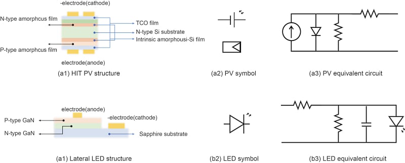
Figure 1. Structure, symbol, and equivalent circuit of photovoltaic battery ( HIT ) and LED. Image used courtesy of Bodo’s Power Systems [PDF]
A typical photovoltaic cell (PV) output current is expressed as:
\[i=i_{sc}-i_{DO}\cdot{\Big(}e\frac{q(V+i\cdot R_{S})}{AKT}-1{\Big)}-\frac{V+i\cdot R_{S}}{R_{P}}\]
Where:
isc -Excitation current produced by light irradiation;
iDO -Saturation current of PN junction;
q -Electron’s charge as 1.6x10⁻¹⁹ C;
K -Boltzmann constant as 1.38X10⁻²³J/K;
A -Ideal constant between 1~2; T -Temperature of PN junction.
Besides, different switching FETs and diode semiconductors such as MOS, gallium nitride (GaN), silicon carbide (SiC), and IGBT are used with different advantages in cost and performance under different application conditions.
Grid-connected Solar Power Generation
Grid-connected solar power generation needs to meet specific technical requirements, such as IEEE1547(US.) ENEL 2010 Ed.2.1 (Italy), EN50438 (European) and GB/T 19939-2005, GB/Z 199642005 (China).To configure an appropriate grid-connected inverter, the photovoltaic system needs multi-stage power conversion, efficiency control, and complete monitoring associated communication system, with necessary functions such as islanding detection and power yield prediction. Typical off-grid and grid-connected photovoltaic power generation systems are shown in Figure 2.
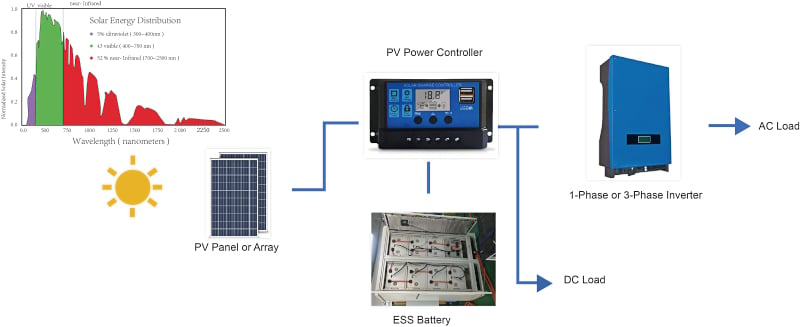
Figure 2. Typical off-grid photovoltaic power generation systems. Image used courtesy of Bodo’s Power Systems [PDF]
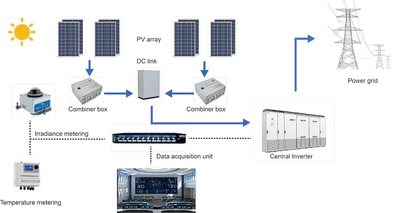
Figure 3. Typical off-grid photovoltaic power generation systems. Image used courtesy of Bodo’s Power Systems [PDF]
Safety is more important than efficiency to be considered in grid-connected photovoltaic power generation systems, which mainly includes islanding detection, insulation detection, leakage current detection, LVRT and etc.
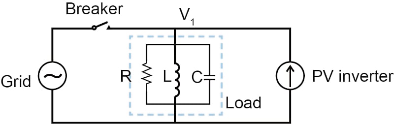
Figure 4. Principle of islanding detection for grid-connected PV power generation (simplified). Image used courtesy of Bodo’s Power Systems [PDF]
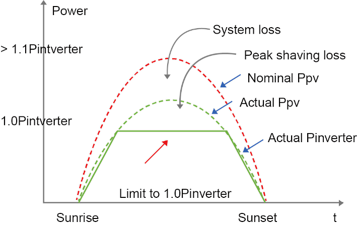
Figure 5. Principle of islanding detection for grid-connected PV power generation (simplified). Image used courtesy of Bodo’s Power Systems [PDF]
Power Conversion Types in Photovoltaic Power Generation
Photovoltaic power generation has a fluctuating relationship between its power output and its working voltage. That is, in the actual power conversion, control of the maximum power output needs to be realized first.
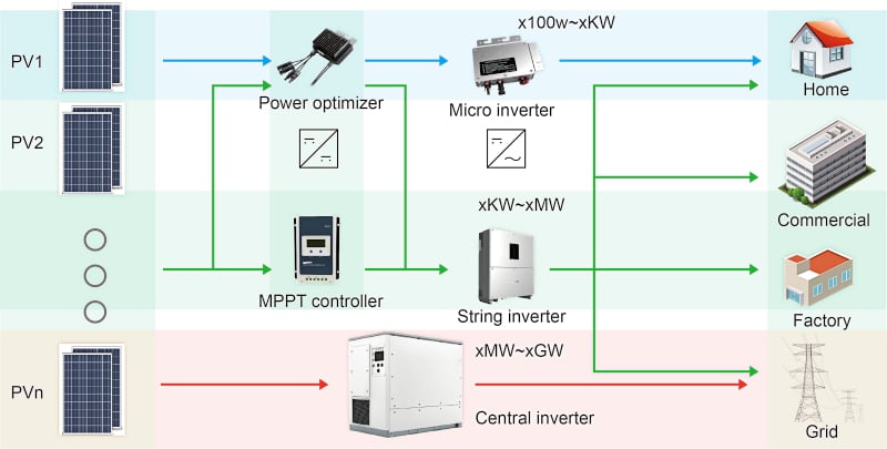
Figure 6. Power conversion in PV power generation: (Blue) Micro-inverter (Green) String inverter (Red) Centralized inverter. Image used courtesy of Bodo’s Power Systems [PDF]
Magnetics Applications in Solar Energy
MPPT (or Power Optimizer)
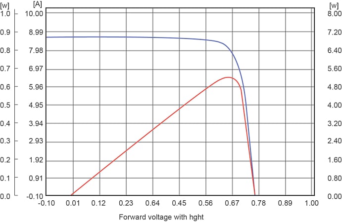
The development of photovoltaic cells has gone through several technical iterations. In the latest 6.0 era represented by 210 cells (210mmx210mm), a single chip power output of 10~12 W can be achieved at an irradiation intensity of 1000 W/m2 at 25°C.
Usually, the specification of the PV will provide the open circuit voltage (VOC), short circuit current (ISC), voltage of maximum power point (Vmp), as well as maximum power point current (Imp).
\[FF(\%)=\frac{V_{mp}\cdot I_{mp}}{V_{oc}\cdot I_{sc}}\]
Figure 7. 210 PV cell- (a) I-V curve (b) Specification (TW SolarTW210y212A (half-type PV cell))
| Code | Eff% | Pmpp (w) | Vmpp (v) | Impp (A) | Voc (V) | Isc (A) | FF% |
| TW-210M-250 | 25.00 | 5.51 | 0.675 | 8.166 | 0.7487 | 8.573 | 85.89 |
| TW-210M-249 | 24.90 | 5.49 | 0.674 | 8.145 | 0.7484 | 8.560 | 85.78 |
| TW-210M-248 | 24.80 | 5.47 | 0.673 | 8.123 | 0.7482 | 8.554 | 85.47 |
| TW-210M-247 | 24.70 | 5.45 | 0.672 | 8.116 | 0.7478 | 8.553 | 85.24 |
| TW-210M-246 | 24.60 | 5.43 | 0.671 | 8.093 | 0.7472 | 8.542 | 85.11 |
| TW-210M-245 | 24.50 | 5.41 | 0.670 | 8.076 | 0.7470 | 8.541 | 84.80 |
| TW-210M-244 | 24.40 | 5.39 | 0.668 | 8.061 | 0.7469 | 8.541 | 84.46 |
| TW-210M-243 | 24.30 | 5.37 | 0.667 | 8.046 | 0.7465 | 8.536 | 84.24 |
| TW-210M-242 | 24.20 | 5.35 | 0.666 | 8.033 | 0.7461 | 8.530 | 84.01 |
| TW-210M-241 | 24.10 | 5.32 | 0.664 | 8.024 | 0.7456 | 8.526 | 83.76 |
| (b) TW Solar-TW210Y212A(half-type PV cell) specification | |||||||
Although MPPT can be implemented in various ways, from the circuit form, the adjustment mode is basically realized by the Boost circuit.
\[U_{pv}=V_{o}\cdot(1-DC)\]
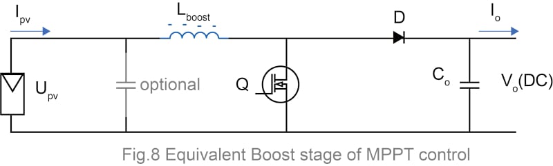
Figure 8. Equivalent Boost stage of MPPT control. Image used courtesy of Bodo’s Power Systems [PDF]
The boost inductance Lboost required by the MPPT control should meet the requirement that the converter circuit is in CCM operation (continuous inductor current mode), so that the PV can operate in the best state and the input bypassing capacitor can be reduced at the same time. The inductance value should be large enough to reduce the influence of switching FET-Q in MPPT control.
\[L_{boost}\geq\frac{V_{o}\cdot DC_{min}\cdot(1-DC_{min})^{2}}{2f_{sw}\cdot I_{o\,min}}\]
Eg.1: When ignoring conversion efficiency, if the DC-link will supply an inverting power of 700Vx1A, the maximum power the PV installation can support is at 700W = 170Vx4.12A, switching frequency is 20 KHz, if the open circuit voltage of the PV cell is Uoc = 195V, then:
\[DC_{min}=1-\frac{U_{oc}}{V_{o}}=1-\frac{195}{700}=72.1\%\]
The corresponding minimum inductance required is:
\[L_{boost}\geq\frac{700\cdot72.1\%\cdot(1-72.1\%)^{2}}{2\cdot20\cdot10^{3}\cdot1}\approx982\mu H\]
The maximum inductor current is:
\[I_{L\,max}=4.12+\frac{1}{2}\cdot{\Big(}\frac{170\cdot0.757}{20.10^{3}\cdot982\cdot10^{-6}}{\Big)}=7.4\,A\]
The RMS value of inductor current is:
\[I_{L\,rms}=\sqrt{4.12^{2}+\frac{1}{12}\cdot(\frac{170\cdot0.757}{20\cdot10^{3}\cdot982\cdot10^{-6}})^{2}}\approx4.53\,A\]
Accordingly, the parameters required for the boost inductor can be defined as 1mH, saturation current 9A, and temperature-rise current 7A (40K temperature rise) with appropriate margins.
For the boost inductor, the maximum voltage at both ends is the higher value between Vo – Upv and UOC, which is 530V and, therefore, can be set to 600V. For PV terminal circuits, the Category II transient overvoltage range is defined in IEC 62109-1 and is suitable for 2500Vdc transient overvoltage, so the 1.6mm clearance (e.g., Pin to pin distance) needs to be met.
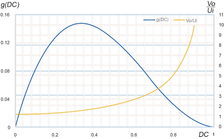
Figure 9. Inductance requirement for boost inductor and voltage gain versus Duty cycle (DC%). Image used courtesy of Bodo’s Power Systems [PDF]
The relationship between the inductance value and DC% is preset in the above minimum inductance value requirement for the boost inductor, determined by g(DC) = DC · (1 – DC)2 Figure 8 shows the influence of DC% on inductance requirement and its simultaneous influence on voltage gain \(\frac{V_{o}}{U_{i}}\).
The main available switching FETs and Diodes can be divided into three categories: MOS, SiC, and GaN, the main applicable voltage ranges are shown in Figure 9.
Figure 10. Comparison of the applicable range of different types of switching FETs
| Comparison between different FETs | MOSFET | SJ-FET(MOS) | SiC | GaN | IGBT |
| Switching freq.(KHz) | ~100 | ~500 | 20~600 | 50~20000 | ~20 |
| Rail voltage.(V) | ~60 | ~600 | 600~1000 | ~600 | 600~1500 |
| Blocking voltage.(V) | 60~150 | ~600 | 600/650/1200 | 600/650 | 650/950/1200/1500 |
| Applicable power.(W) | ~x.KW | ~x.10KW | 1~x.100KW | ~10KW | 1~1MW |
| Benefit | Cost-effective | High switching req. | Better thermal resistivity | 50% less switching loss than SiC | High volt. & low Rdson. |
Eg.2: When ignoring conversion efficiency, if the DC-link supplies an inverting power of 400Vx2A, the maximum power the PV installation can support is 800W = 60Vx13.33A. Switching frequency is 100KHz, and if the open circuit voltage of the PV cell is Uoc = 70V, then:
\[DC_{min}=1-\frac{U_{oc}}{V_{o}}=1-\frac{70}{400}=82.5\%\]
The corresponding minimum inductance required is:
\[L_{boost}\geq\frac{400\cdot82.5\%\cdot(1-82.5\%)^{2}}{2\cdot100\cdot10^{3}\cdot2}\approx25.3\mu H\]
The maximum inductor current is:
\[I_{L\,max}=13.33+\frac{1}{2}\cdot(\frac{60\cdot0.825}{100\cdot10^{3}\cdot25.3\cdot10^{-6}})^{2}=23.11A\]
The RMS value of inductor current is:
\[I_{L\,rms}=\sqrt{13.33^{2}+\frac{1}{12}\cdot(\frac{60\cdot0.825}{100\cdot10^{3}\cdot25.3\cdot10^{-6}})^{2}}\approx14.48A\]
When considering the inductor design, choose a limited package size, because the ripple current ratio is:
\[a\%=\frac{60\cdot0.825}{100\cdot10^{3}\cdot25.3\cdot10^{-6}}\cdot\frac{1}{13.33}=147\%\]
Taking Eg. 2 as an example, assuming the effective cross-sectional area provided by the selected magnetic core is Ae and the effective magnetic circuit length is Le. If the maximum inductor current allowed at minimum inductance is its saturation current, its maximum working flux density is:
\[B_{max}=\frac{L_{sat.}\cdot(1+\frac{1}{2}a)\cdot13.33A}{N\cdot A_{e}}\]
And the minimum working flux density is:
\[B_{min.}=\frac{L\cdot(1-\frac{1}{2}a)\cdot13.33A}{N\cdot A_{e}}\]
According to the core loss \(P_{cv}(\frac{mw}{cm^{3}})\) curve, the core loss will be approximated as:
\[P_{cv}=K\cdot f^{a}\cdot B^{b}(f:KHz;B:KGauss;K,a,b\,provided\,by\,manufacturer)\]
\[P_{cv\,op}=P_{cv\,Bmax.}-P_{cv\,Bmin.}\]
\[P_{core}=\frac{1}{2}P_{cv\,op}\cdot A_{e}\cdot l_{e}\,(mW)\]
Here, "the maximum allowable inductor current at a minimum inductance it its saturation current." However, this is not always the case. In an actual working circuit, as long as the guaranteed maximum current placed in the core material under the DC Bias curve is far from its saturation point, just check the following relationship if it is satisfied or not:
\[H_{op}(Oersted)\leq H_{-30\%\,of\,\mu _i}\]
Therefore, it is more like an additional design margin that is taking the maximum possible power loss for evaluation. Besides the core loss, the copper loss will be approximated, with only the skin effect being considered for preliminary evaluation:
\[P_{cu}=I_{L\,rms}^{\,\,\,\,\,\,\,\,\,\,\,\,\,\,2\,}\cdot ESR\]
Taking the example of CODACA inductor CPER3231-101MC for Eg.2, the specifications listed below are key parameters with manufacturer definitions:
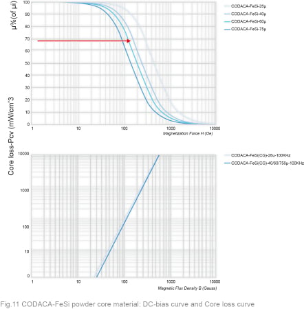
Figure 11. CODACA-FeSi powder core material: DC-bias curve and Core loss curve. Image used courtesy of Bodo’s Power Systems [PDF]
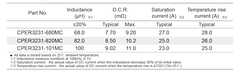
Image used courtesy of Bodo’s Power Systems [PDF]
The corresponding ripple current will be:
\[I_{ripple}=\frac{60\cdot0.825}{100\cdot10^{3}\cdot100\cdot10^{-6}}=4.95A\]
The maximum inductor current is:
\[I_{L\,max}=13.33+\frac{1}{2}\cdot(4.95)=15.8A\]
When inductance drops by 30%, the ripple current will rise 43% and it will be 4.95x1.43 = 7.07 A, the corresponding maximum current will be \(13.33+\frac{7.07}{2}=16.87 A\). It is smaller than spec. (23A), so the above estimation could be taken as a maximum loss condition. The power loss calculation follows as:
\[B_{max}=\frac{L_{sat.}\cdot(1+\frac{1}{2}a)\cdot13.33A}{N\cdot A_{e}}=\frac{100\cdot10^{-6}\cdot0.7\cdot16.87}{25.5\cdot1.523\cdot10^{-4}}=3.04KGauss\]
\[B_{min}=\frac{L_{sat.}\cdot(1+\frac{1}{2}a)\cdot13.33A}{N\cdot A_{e}}=\frac{100\cdot10^{-6}\cdot0.7\cdot10.86}{25.5\cdot1.523\cdot10^{-4}}=2.796KGauss\]
\[P_{cv\,op}=P_{cv\,Bmax.}-P_{cv\,Bmin}=1.79\cdot100^{1.5}\cdot(3.04^{2.03}-2.796^{2.03})\approx2672\,mW/cm^{3} \]
\[P_{core}=\frac{1}{2}P_{cv\,op}\cdot A_{e}\cdot l_{e}=\frac{1}{2}\cdot2672\frac{mW}{cm^{3}}\cdot1.523cm^{2}\cdot7.99cm=16.26W\]
The RMS value of inductor current is now:
\[I_{L\,rms}=\sqrt{13.33^{2}+\frac{1}{12}\cdot(4.95)^{2}\approx13.4A}\]
\[P_{cu}\approx13.4^{2}\cdot9.02\cdot10^{-3}\approx1.62W\]
Thus, the total loss is 17.88W and the efficiency loss is approximately 2.24%.
In order to achieve a lower loss, within the limited package size, it is necessary to increase the inductance value as much as possible in order to exchange for a lower ripple current amplitude.
In this example, the saturation current and temperature-rising current are still high, and space is left for adjusting the number of turns and permeability to meet the requirements for optimal loss: adjustments are made on the basis of existing products: increase the coil turns to N=38.5, and the permeability is reduced to maintain the same L value: (the actual available material is standard 40ur)
\[\mu_{r\,adjusted}=90\cdot{\Big(}\frac{25.5}{38.5}{\Big)}^{2}=39.5\]
The corresponding DC resistance is adjusted to approximately (based on same volume of copper)
\[R_{dc\,adjusted}=9.02\cdot{\Big(}\frac{38.5}{25.5}{\Big)^{2}}=20.6m\Omega\]
Adjusted power loss as below:
\[B_{max}=\frac{L_{sat.}\cdot(1+\frac{1}{2}a)\cdot13.33A}{N\cdot A_{e}}=\frac{100.10^{-6}\cdot0.7\cdot16.87}{38.5\cdot1.523\cdot10^{-4}}=2.014KGauss\]
\[B_{min}=\frac{L\cdot(1+\frac{1}{2}a)\cdot13.33A}{N\cdot A_{e}}=\frac{100\cdot10^{-6}\cdot10.86}{38.5\cdot1.523\cdot10^{-4}}=1.852KGauss\]
\[P_{cv\,op}=P_{cv\,Bmax.}-P_{cv\,Bmin}=1.79\cdot100^{1.5}\cdot(2.014^{2.03}-1.852^{2.03})\approx1160\,mW/cm^{3}\]
Verify if the core is saturated or not:
\[H_{max}=\frac{N\cdot I_{L\,max.}}{l_{e}}=\frac{38.5\cdot 16.87\cdot4\pi}{7.99\cdot10^{-2}\cdot10^{3}}\approx102.2Oe\]
The core saturation can be determined by the DC-bias curve of the core. The calculation is valid because the core has not reached the saturation point. Then the power loss after adjustment is:
\[P_{core}=\frac{1}{2}P_{cv\,op}\cdot A_{e}\cdot l_{e}=\frac{1}{2}\cdot1160\frac{mW}{cm^{3}}\cdot1.523cm^{2}\cdot7.99cm=7.1W\]
\[P_{cu}\approx13.4^{2}\cdot20.6\cdot10^{-3}\approx3.7W\]
Now the total loss is 10.8W and the efficiency loss is 1.35%. Still, based on: 1, the core is still far away from the saturation point after decreasing permeability; 2. The relative ratio of copper wire loss is still not high, and the inductor can continue to optimize the loss by increasing the number of turns and decreasing the permeability or leveraging the package size and going with a higher inductance value.
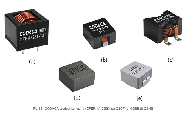
Figure 12. CODACA product series: (a)CPER (b)CSBX (c)CSCF (d)CSEB (f) CSHB. Image used courtesy of Bodo’s Power Systems [PDF]
Micro-inverter PV applications often plug into local energy storage cells to achieve optimal wave equalization of power, so that the voltage of the DC bus can be adjusted according to the connected battery series, such as 12 V, 24 V, 48 V or a higher battery pack voltage. Such applications generally use flat copper wire wound inductors or even molded inductors at lower power levels.
Other Magnetics in Photovoltaic Power Generation Applications
MPPT for the isolation of photovoltaic inverter application (micro power inverter), flyback or full bridge ZVS soft switching topology, correspondingly needs a design power transformer and an LLC resonant inductor; the material of the magnetic core selection generally will utilize an MnZn ferrite (air gap) to reduce the power loss.
In distributed photovoltaic applications, isolators adopting dielectric isolation are prioritized to drive the corresponding switch FETs. The gate drive transformer is basically independent and needs to be designed according to the corresponding application. In the inverter phase, filter inductors with large inductance and large volume, also known as ACL, are usually configured to correspond to DCL inductors used for PV terminal input to reduce switching noise and isolate the noise path between the PV power generation terminal and the power grid.
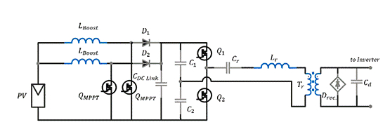
Figure 13. Interleaving boost MPPT plus half-bridge LLC resonant conversion. Image used courtesy of Bodo’s Power Systems [PDF]
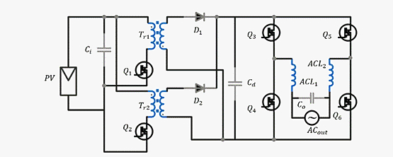
Figure 14. Full-bridge flyback MPPT plus full-bridge inverter for AC output. Image used courtesy of Bodo’s Power Systems [PDF]
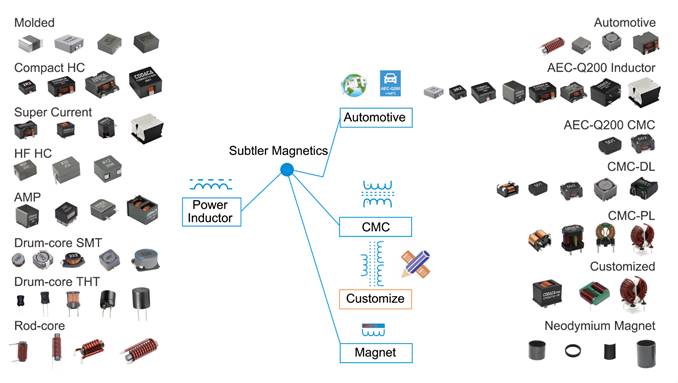
Figure 15. CODACA product lines by September 2022. Image used courtesy of Bodo’s Power Systems [PDF]
About CODACA
Founded in 2001, Shenzhen CODACA Electronics Co., LTD. (CODACA), has been actively engaged in R&D magnetics for serving global solar energy clients integrating several product line series into automotive components, high current inductors, and molded inductors details, please see Figure14.
To help customers in photovoltaics effectively calculate inductor losses and simplify the selection of magnetics, CODACA offers an online loss calculation tool and several product comparison screening tools.
References
[1] Infineon Technologies AG. Exploiting the unlimited potential of Solar energy – Trends and solutions
[2] CODACAPower Inductor product information
[3] Dave Freeman. Introduction to Photovoltaic Systems Maximum Power Point Tracking
[5] Trina Solar. Trina Solar Vertex Magic Box PV Inverter White Paper
[6] STMicroelectronics. The right technology for solar converters, AN3152
[7] Texas Instruments Incorporated. Demystifying high-voltage power electronics for solar inverters
[8] MPS. Comparative Study of PFC Topologies: Interleaved Boost vs. Totem-Pole PFC Topologies
[10] Huawei. SUN2000-3/4/5/6KTL-L1 Smart Energy Controller
[12] SMA. SMA-40years-Booklet-zh.pdf
This article originally appeared in Bodo’s Power Systems [PDF] magazine.
Featured image used courtesy of Adobe Stock