Facebook
 Google
 GitHub
 Linkedin
Examining Vertical GaN Power ICs
This article examines how Fraunhofer is combining lateral and vertical geometry to develop vertical GaN power ICs and related technology.
This article is published by EEPower as part of an exclusive digital content partnership with Bodo’s Power Systems.
Two trends have emerged in GaN power technologies. On the one hand, the monolithic integration of system peripherals to the power transistor can reduce system and bill of materials costs and improve performance. On the other hand, vertical transistors are being developed to increase breakdown voltages and achieve higher switching power. Combining lateral and vertical geometry is the aim of Fraunhofer IAF with the development of vertical GaN power ICs and related technology.
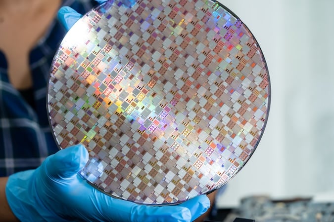
Image used courtesy of Adobe Stock
Combining Lateral and Vertical Geometry for GaN ICs
Combining the best of both worlds is the motto behind the development of vertical GaN power ICs.
The lateral GaN technology, with its HEMT design, has revolutionized the field of power electronics offering significant performance advantages and increasingly lower costs compared to conventional Si-based power transistors. Lateral structures can integrate active or passive devices to the GaN power HEMT on-chip, enabling functions like gate drivers, sensing, or protection circuits—known as a GaN power IC or GaN power integration. However, commercial lateral GaN transistors have a limited breakdown voltage of typically 650 V (in some cases even 1200 V) and a switching power capability of a few kilowatts.
The aim is to overcome these limitations with vertical GaN transistors, which also have the advantage of increasing the breakdown voltage without enlarging the chip size. Furthermore, the reliability and thermal management can be improved by moving the peak electric field and dissipation of heat from the surface into the bulk substrate. There are four major vertical GaN device approaches such as trench MOSFET, FinFET, JFET, and CAVET (current aperture vertical electron transistor). Toyota, Panasonic, or start-ups like Oddysey Semiconductor and the recently dissolved NexGen Power Systems have demonstrated promising normally-off vertical GaN transistors, but they are not yet commercially available.
One of the biggest challenges facing vertical GaN devices is their economic viability, mainly due to the high cost of GaN wafers. Today, 6-inch GaN substrates are under development, while 2- and 4-inch are in mass production, but the cost of a wafer, including epitaxial layers, is currently high at 40-60$/cm2 compared to ~7$/cm2 for 4-inch SiC or ~1$/cm2 for 8-inch GaN-on-Si. This relatively high price must be reduced to ensure the breakthrough of vertical GaN transistors despite a theoretical improvement in the unipolar RON×A figure-of-merit compared to SiC MOSFETs. In vertical device structures, only the CAVET features the same heterostructure as the conventional HEMT with the same gate module. While different epitaxial layers are used as vertical depletion zones, the process technology can be widely adopted from the known lateral devices. This unique selling point of the CAVET opens a way to continue lateral GaN power integration in vertical device concepts to a vertical GaN power IC (Figure 1) and could become a promising vertical structure of the future.
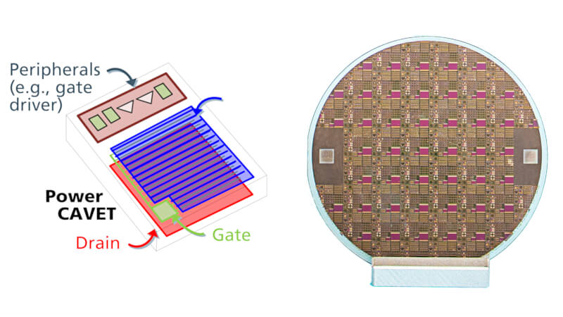
Figure 1. a) 3D view of a vertical GaN power IC and b) photograph of a fully processed 2-inch GaN-on-GaN wafer. Image used courtesy of Bodo’s Power Systems [PDF]
Co-Integration of Lateral HEMTs and Vertical Power CAVET
Fraunhofer IAF has developed a technology that combines a co-integrated large-area vertical GaN power transistor with lateral devices to realize peripheral functions on a single chip. The CAVET combines a well-known gate module of the lateral HEMT with a vertical depletion- and drift-zone. Consequently, the same normally-off concepts used for the HEMT (e.g., pGaN gate) can be applied to the CAVET. This technology starts with a highly negatively doped (n+) GaN substrate and subsequent homoepitaxy, which has significantly better dislocation densities than heteroepitaxy on foreign substrates such as Si or Sapphire and can therefore positively influence breakdown voltage and reliability. With the help of MOCVD (metal-organic chemical vapor deposition), a weaker n-doped (n-) GaN layer with a few micrometers is grown on top, which serves as a depletion- and drift-zone. A positively doped (p) GaN current blocking layer (CBL) is then manufactured by Mg-implantation, which acts as an insulating layer separating the source from the drain. At the same time, an aperture allows vertical current flow below the gate area. Finally, an un-intentionally doped (uid)- GaN channel, an AlGaN heterostructure, and a GaN cap or alternatively p-GaN are regrown above, which build the access region of the vertical transistor and the channel region of the lateral HEMTs. The devices are fabricated in a III-V process line. The same active and passive components as in the lateral GaN technologies are available. Figure 1b shows a fully processed 2-inch GaN-on-GaN wafer, which could also be realized on larger diameters in the future. A simplified cross-section of the technology and a TEM cross-sectional image of a fabricated CAVET are shown in Figures 2a and c).
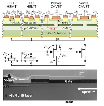
Figure 2. CAVET technology with quasi-monolithic integrated HEMT gate driver stage and sense CAVET as a) simplified cross-section and b) corresponding circuit diagram. c) TEM image of a section of the vertical CAVET device marked in red in a). Image used courtesy of Bodo’s Power Systems [PDF]
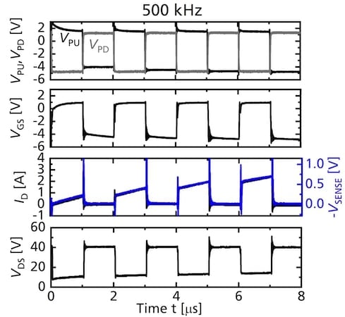
Figure 3. Switching measurement of the power CAVET device controlled by lateral co-integrated HEMTs and sense CAVET at 500 kHz and 40 V. Image used courtesy of Bodo’s Power Systems [PDF]
Experimental Results
To demonstrate the development of vertical GaN power ICs, several vertical and lateral devices were manufactured with the same technology. After processing, the components were diced for flexibility. Still, they should behave like monolithically integrated on one die/chip if the backside or drain potential DC is the same or connected together (circuit diagram in Figure 2b). The experimental proof-of-concept uses a large-area CAVET power device controlled by a quasi-monolithically integrated lateral HEMT push-pull driver stage with current sensing via a sense CAVET. Figure 2b shows the corresponding circuit diagram/symbols and indicates the current direction (lateral vs. vertical) by the orientation of the symbols. The push-pull HEMT stage consists of a pull-up/down (PU/PD) transistor, and the current-mirror ratio N is ~229.
The GaN-based devices were statically characterized in detail. The dynamic switching measurements are carried out in a double-pulse test setup at 40 V, up to 2.4 A, and 500 kHz, and the gate-source voltage of the PU/PD device VPU/VPD, the gate-source voltage of the power CAVET VGS, which corresponds to the VGS of the sense CAVET, the drain-current ID and drain-source voltage VDS of the power CAVET are shown in Figure 3. The drain current of the power CAVET is measured by a voltage drop of a coaxial shunt and the mirrored current through the sense transistor is converted into the voltage VSENSE using an external trans-impedance amplifier.
Takeaways
The development of vertical GaN power ICs aims to merge the benefits of lateral GaN technology with a vertical transistor structure. Not only traditional parameters such as higher voltage and current should be addressed, but also the advantage of monolithic functional integration and the associated reduction in system costs. This is intended to provide a further sales argument for the vertical GaN transistors, which are currently still in an early development state and commercially rarely available. However, the research results show their great potential. Vertical GaN power ICs will push the performance of this technology even further and will be continued in ongoing projects at Fraunhofer IAF.
This article originally appeared in Bodo’s Power Systems [PDF] magazine and is co-authored by Michael Basler, Richard Reiner, Stefan Mönch, and Philipp Döring, Fraunhofer Institute for Applied Solid State Physics (Fraunhofer IAF).