Facebook
 Google
 GitHub
 Linkedin
Space-Saving WBG Devices Deliver Power, Efficiency
The latest SiC and GaN devices offer superior performance for various applications, paving the way for the next wave of technological advancements.
Gallium nitride (GaN) and silicon carbide (SiC) are pushing the boundaries of power electronics with their superior performance characteristics compared to traditional silicon devices. Their properties make them ideal for next-generation GPUs and data center power supplies. Their higher efficiency reduces energy consumption, decreasing cooling requirements and operational costs. Furthermore, their higher power density allows for cramming more processing power into smaller physical spaces, which is crucial for data center optimization.
Advancements in packaging and manufacturing processes have further propelled the adoption of SiC and GaN devices. Developers have created packages that can handle the high voltages while maintaining compactness. Additionally, advancements in manufacturing processes give lower on-resistance to improve efficiency and power density.
Several new wide-bandgap devices targeting diverse applications offer enhanced performance for upcoming technologies.

Data center servers. Image used courtesy of Adobe Stock
Infineon's Latest CoolSiC and CoolGaN MOSFETs
Infineon continues its CoolSiC MOSFETs series to cater to applications below 650 V. The 400 V family is specially developed for AC-DC stages in artificial intelligence (AI) servers. Moreover, the MOSFETs also address applications in solar and energy storage systems, inverter motor controls, industrial and auxiliary power supplies, and solid-state circuit breakers for residential buildings. They are based on Infineon's second-generation trench MOSFET technology, which offers ultra-low conduction and switching losses compared to existing 650 V SiC and Silicon MOSFETs.
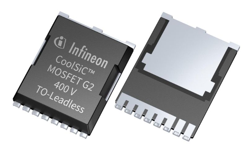
Infineon’s 400 V CoolSiC MOSFETs. Image used courtesy of Infineon
An AI server PSU's AC/DC stage implemented in a multi-level PFC using CoolSiC MOSFETs can achieve a power density of more than 100 W/in3 and reach 99.5% efficiency. The AI server PSU's DC/DC stage can utilize CoolGaN transistors to provide over 8 kW power output, with three times the power density compared to existing solutions.
Infineon also released two new generations of high- and medium-voltage CoolGaN devices built on 8-inch foundry processes for 40 V to 700 V voltage classes. The new gallium nitride MOSFETs target consumer, data center, industrial, and solar uses.
Improved Package for Nexperia SiC MOSFETs
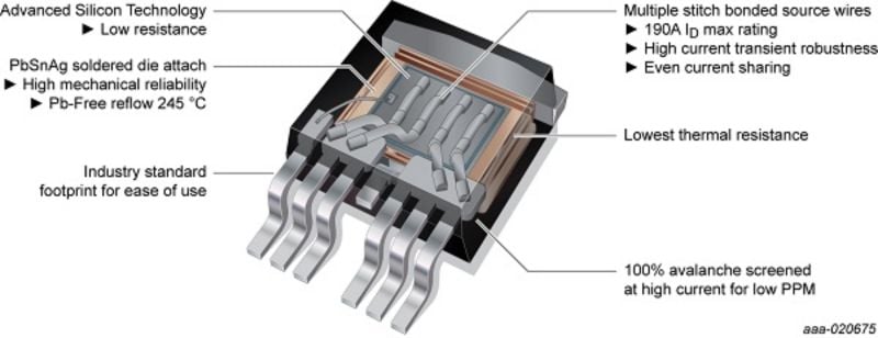
Nexperia will offer its popular 1200 V SiC MOSFETs in D2PAK-7 surface mount device packaging with 30, 40, 60, and 80 mΩ on-resistance values. The on-resistance (RDS(on)) of a SiC MOSFET can vary significantly due to several factors, including the device design, manufacturing process, and operating conditions. With the new packaging, the on-resistance in Nexperia’s SiC MOSFETs only increases by 38% over an operating temperature ranging from 25°C to 175°C.
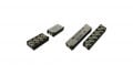
D2PAK-7 packaging. Image used courtesy of Nexperia
When connecting power MOSFETs in parallel, variations in threshold voltage (Vth) can lead to imbalanced current sharing among the devices. The MOSFET carrying more current will heat up more. As Vth decreases with increasing temperature, the hotter MOSFET will continue to draw more current, exacerbating the imbalance and creating a thermal runaway. Nexperia SiC MOSFETs have extremely tight threshold voltage specifications to offer a balanced current performance. Moreover, their low body diode forward voltage increases efficiency and robustness while relaxing the dead-time requirement during freewheeling.
Compact Half-Bridge MOSFETs for DC-DC Applications
Alpha & Omega Semiconductor Limited unveiled its AONG36322 XSPairFET, featuring two 30 V MOSFETs in a half-bridge configuration, with the high-side and low-side MOSFETs in an asymmetric DFN3.5x5 XSPairFET package. The company claims its solution is ideal for space-constrained DC-DC applications like point-of-load computing, USB hubs, and power banks. The new MOSFET pair replaces the existing DFN5x6 asymmetric package to increase compactness by 60%.
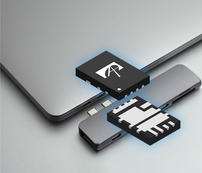
AONG36322 half-bridge MOSFETs for compact DC-DC solutions. Image used courtesy of Alpha & Omega Semiconductor
Their latest bottom-source packaging technology allows for high-side and low-side MOSFETs to offer ultra-low 4.5 m Ω and 1.3 mΩ maximum-on-resistance, respectively. In addition, the new packaging reduces parasitic inductance and, in turn, reduces switch node ringing.