Facebook
 Google
 GitHub
 Linkedin
MOSFET Innovations for Increasing the Power Density of Auto Electronics
Vehicle electrification reduces carbon footprints compared to traditional cars, but the increased electronics require more electrical power to operate, requiring a more extensive network of power supplies operating at high power density and efficiency.
As MOSFETs provide critical switching functions in power management designs, choosing a device with an optimized balance of physical, thermal, and electrical attributes is critical to increasing power density. The latest innovations in power MOSFET packages elevate performance and provide ruggedness in extremely compact form factors.

Image used courtesy of Adobe Stock
On-Resistance Minimization
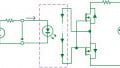
Legacy transistor outline (TO) packages have provided proven solutions for powertrain applications that require power ratings from several hundred to thousands of watts. Products in TO packages often use aluminum (AI) wires to connect the “source” of the MOSFET’s silicon to the terminals. This type of construction has its limitations, particularly for the latest technologies, which have very low RDS-Area.
For example, the most advanced 40 V device in a 7-pin D2PAK with Al wires will have a 33 % to 67 % split between silicon- and package-contributed resistance. Thus, the intrinsic limitation hinders the creation of better MOSFET products.

Image used courtesy of Vishay
As the semiconductor industry continues reducing the RDS-Area of technologies, the package also requires innovation to better complement the silicon. The new package constructions replace Al wires with bond-wireless (BWL) interconnection for surface-mount packages. In the BWL architecture, the source and gate of the MOSFET are connected to the terminals by two metal clips. This dual-clip construction is optimized through finite element analysis to reduce stress on the die and leads while minimizing resistance and inductance.

Image used courtesy of Vishay
The source clip effectively expands the cross-sectional area for conducting electrical current, enabling a package resistance as low as 0.1 mΩ, which reduces the package’s contribution to total resistance to 23 % or less. Combined with the latest silicon, low-voltage devices can easily achieve RDS(ON) in the micro-ohm range.

Image used courtesy of Vishay
The metal source clip also acts as a heat slug to improve the thermal transfer of the package. In addition, the wafers used for BWL packages are ground to 50 µm thick to achieve lower RDS(ON) and superior thermal performance.

Image used courtesy of Vishay
Increased Performance and Efficiency
Due to P = I2*R, the power loss (P) from conduction for a given current (I) can be reduced by having low RDS(ON) values. As power loss heats up the junction temperature, the RDS(ON) rises as the device becomes hotter. Reducing power loss allows the device in a BWL package to stay cooler and prevents RDS(ON) from increasing quickly with more load current.

Image used courtesy of Vishay
As the BWL construction minimizes the overall resistance, the best 40 V device in an 8 mm x 8 mm package is 40°C cooler than the best D2PAK product in our portfolio. In addition, the smaller package occupies less PCB real estate and helps achieve higher power density.

Image used courtesy of Vishay
For powertrain applications, such as liquid pumps or power steering, lower conduction loss translates into cooler operating temperatures and reduces the complexity of thermal management systems to save costs.
PCB Footprint Reduction and Enhanced Board-Level Reliability
The BWL construction is currently qualified in various surface-mount package types, including the PowerPAK 8x8L, 8x8LR, SO-8L, and 1212-8SLW. These packages have exposed drain pads on either the bottom or top side to allow for better thermal transfer. The typical footprints of these packages range from 80.34 mm2 for the 8x8LR to 10.89 mm2 for the 1212-8SLW.
Designing with PowerPAK packages requires less PCB real estate for MOSFETs than legacy TO packages. High-power applications above the kilowatt level usually need multiple large die MOSFETs such as D2PAKs. These TO packages are at least 160 mm2 and take up significant board space when configuring them in parallel. In comparison, the PowerPAK 8x8L has only a footprint of 64.8 mm2. The benefits of a small size and lighter package weight become even more significant when several tens of devices are situated on the PCB.
The top-cooled PowerPAK 8x8LR has a slightly larger package footprint of 83.36 mm2, and the package occupies 50 % less PCB real estate than the D2PAK. The exposed drain pad on top of the package allows heat to migrate upward directly to the heatsink or enclosure.

Image used courtesy of Vishay
One distinctive feature of the new PowerPAKs is their gullwing-shaped leads, which are designed for maximum stress relief and superior board-level reliability. During the development stage, the packages went through rigorous aging and stress tests, such as power temperature cycling or vibrational testing on test boards. The proprietary mold compound for encapsulation features customized properties to minimize CTE mismatches and reduce stress from thermal cycling. The gullwing leads are engineered for maximum mechanical stress relief. Therefore, this package is built to achieve high board-level reliability and can reduce the return rate.

Mold compound features customized properties to reduce stress for board-level reliability. Image used courtesy of Vishay
Top-Side Cooled Packages
Select powertrain applications that operate at high currents often need to utilize the metal enclosure or heatsinks to remove heat generated by the power loss of components. To leverage such a thermal management design, the ideal MOSFET should have an interface with low thermal resistance to meet the heatsink. One solution is the latest PowerPAK 8 x 8 LR package, which provides a top-side cooled feature and is optimized for heatsinking.

Image used courtesy of Vishay
The drain pad is on the top of the encapsulation and provides a direct thermal path from the top of the package to the heatsink, with thermal paste or gap filler at the interface. The heat can escape upward to the heatsink and is directed away from the PCB. As the dominant thermal path is the heatsink, the PCB handles less thermal transfer and can use smaller components, which ultimately lowers the PCB cost. As the heatsink takes away heat more efficiently, the system runs cooler and enables operation at a higher power density.

Image used courtesy of Vishay
For most MOSFET packages with the drain on the bottom side, the heat will be pushed into the PCB through the drain pad and dissipated to the heatsink. This path includes several materials with thermal resistance in series. The PCB area of the MOSFET will also need vias to allow for thermal transfer.
The reverse package also has gullwing leads that are designed for maximum stress relief. The flexibility in the leads allows for expansion and contraction during events of thermal and mechanical stress. While the package exhibits on-resistance as low as 0.54 mΩ (8 x 8 LR, VDS = 40 V), the overall construction is rugged and can lead to high board-level reliability to minimize field returns.
The Takeaway–Smaller, Robust, and More Energy Efficient
The new PowerPAK packages with BWL construction bring out the best of silicon and have lighter weight than devices in comparable TO packages. The resulting products increase efficiency and enable higher power density, so automotive electronic systems can be more energy efficient. The takeaway of the new PowerPAK family includes:
- Significant reduction in PCB real estate
- Minimization of the resistance contributed by the package, with a total RDS(ON) in the micro-ohm range
- Top-cooled PowerPAK optimized for heatsinking, enabling a further reduction of the overall PCB size
- The gullwing-shaped lead design increases the board-level reliability, extending the product lifetime and reducing the chance of failure
With better electrical characteristics and ruggedness, the PowerPAK family increases power density and enhances the reliability of designs.