Facebook
 Google
 GitHub
 Linkedin
Improving Performance With Monolithic GaN Integration While Reducing Size, Cost
This article will examine the advantages of gallium nitride heterojunction field effect power transistors in the 15 V to 350 V range in applications like power conversion, motor drive, and pulsed light for lidar.
This article is published by EE Power as part of an exclusive digital content partnership with Bodo’s Power Systems.
Gallium nitride (GaN) heterojunction field effect power transistors in the 15 V to 350 V range have been shown to give significant advantages over silicon in efficiency, size, speed, and cost in applications such as power conversion, motor drive, and pulsed light for lidar. These advantages are due to the critical electric field being an order of magnitude higher than in silicon, specifically a 3x advantage in the bandgap and a 1.3x advantage in electron mobility.
The resulting devices switch faster, are physically smaller, have lower RDS(on), and can carry a higher inherent current [1]. The majority of today’s GaN transistors have a lateral structure that allows cost-effective integration of many transistors onto a single substrate, as shown in Figure 1 [2].
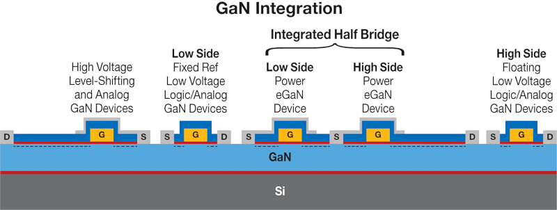
Figure 1. Cross section showing building blocks of a GaN integrated circuit. Image used courtesy of Bodo’s Power Systems [PDF]
Discrete Gate Driver
Each power transistor works intimately with a gate driver as a fundamental building block of power electronic switching converters. For turn-on, the gate driver takes charge from a decoupling capacitor and delivers it to the power transistor’s gate capacitance, with current returning to the decoupling capacitor from the power transistor’s source. For turn-off, the gate driver connects the gate to the source to remove the charge from the gate. The high-transition speed is key to high-frequency operation, and the gate driver must overcome the resistances and inductances of the turn-on and turn-off loops for an efficient solution that works at high frequency. That translates to a strong (low resistance) driver and a low loop inductance.
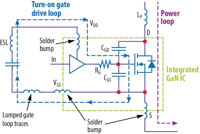
Figure 2 shows the turn-on (a) and turn-off (b) gate drive loops, along with their stray inductances for a discrete solution to the power block. Stray inductances come from traces and interconnections, such as wire bonds, solder bumps, and PCB traces. GaN devices are lateral, with all electrical connections on the same surface, allowing wafer-level packaging with solder bumps. These have much lower inductance than the wire bonds or clips necessary for silicon MOSFETs, which have a vertical structure. A discrete implementation of a GaN transistor with a gate driver has inductances in the equivalent series inductance (ESL) of the capacitor, solder bumps or wire bonds of the gate driver VDD, VSS, and power transistor solder bumps in the gate and source, and PCB traces. These inductances impede the charging and discharging of the power transistor gate capacitance, thus slowing switching and increasing commutation losses.
Of particular concern is Common Source Inductance (LCS). This is the inductance common to the gate drive and power loops. It consists of power transistor source solder bumps and any source PCB traces before the point of separation. It is good design practice to separate these loops as close to the source of the FET as possible. The impact of common source inductance is the power loop di/dt induces a voltage across LCS that subtracts from the VGS applied to the power transistor during turn-on (and adds to the VGS during turn-off), slowing current commutation and increasing switching losses [3][4].
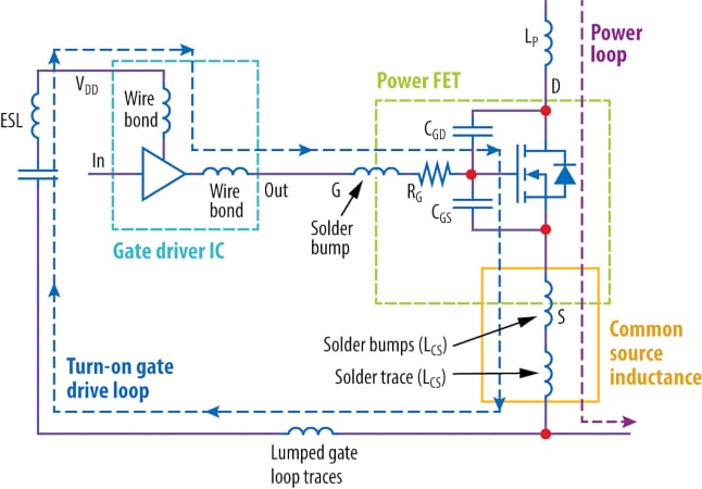
a. Image used courtesy of Bodo’s Power Systems [PDF]
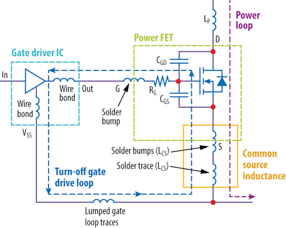
b. Image used courtesy of Bodo’s Power Systems [PDF]
c. Image used courtesy of Bodo’s Power Systems [PDF]
d.
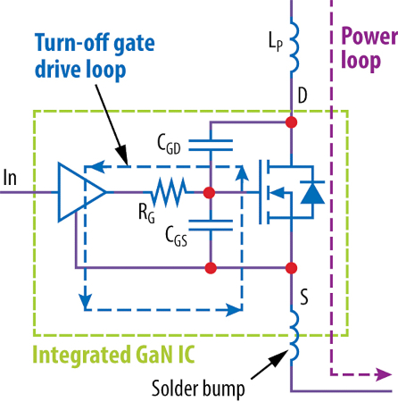
Figure 2. Power block gate drive loops of (a) discrete turn-on, (b) discrete turn-off, (c) integrated GaN turn on, (d) integrated GaN turn-off. Image used courtesy of Bodo’s Power Systems [PDF]
Consider an application like a laser driver for lidar, where turning on 100 A in 1 ns is required. Basic electronics tells us that V = L di/ dt. 50 pH of LCS induces a 5 V leaving 0 V across the gate drive impedance to turn on the power transistor making it impossible to achieve the required di/dt. While this example is extreme, real, common source inductance impact on current commutation time is very significant in power conversion and motor drive applications. Current commutation time is estimated by equation 1 where the gate charge necessary for current commutation is estimated by (QGS - QG(TH)), RG is the lumped gate drive impedance, VGS is the power transistor gate drive voltage necessary to support the commutated current, and VDD is the gate driver voltage.
\(t=\frac{Z_{G}(Q_{GS}-Q_{G(TH)})+L_{CS}I_{D}}{V_{DD}-V_{GS}}\) (1) Current commutation time
\(E=\frac{t*I_{D}*D}{2}\) (2) Energy loss due to current commutation time
\(P=E*f\) (3) Power lost due to current commutation time
As an example, consider EPC2088 [5] hard turn-on, commutating 50 V, 25 A at 1 MHz. QGS = 4.4 nC, QG(TH) = 3.2 nC, ZG = RG (0.4 Ω) plus gate driver resistance of 0.7 Ω (ignoring gate drive loop inductance), VDD = 5 V, VGS @ 25 A = 2.3 V with LCS = 100 pH. The ZG term of equation 1 results in t = 600 ps commutation time. The LCS term results in 1.14 ns current commutation time. In this example, 65% of current commutation time is due to common source inductance. Using equations 2 and 3, 710 µJ of energy is lost in each cycle switching 25 A and 50 V, and 710 mW of power dissipated at 1 MHz due to common source inductance alone. It is clear that minimizing common source inductance is mandatory to enable the size reductions and system benefits of high frequency.
The impact on switching losses from the rest of the gate drive loop inductances is much more straightforward as they are RLC loops where the resistance and inductance impede the charging of the gate capacitance, and if inductance is too high, resistance must be added to control gate overshoot and ringing, further increasing commutation loss. Equation 4 shows the resistance needed for critical damping of the gate loop where RG(on) is the total turn-on gate loop resistance, LG(on) is the turn-on gate loop inductance, Lcs is the common source inductance, and CGS(on) is the FET gate-to-source capacitance at the voltages of commutation [4]. As time, energy, and power scale linearly with common source inductance, power conversion at high frequency require significant attention to packaging and layout.
\(R_{G(on)}\geq\sqrt{\frac{4\times(L_{G(on)}+L_{CS})}{C_{GS(on)}}}\) (4) Resistance necessary for critical damping
Consider an integrated circuit where the power transistor is integrated with the gate driver. This integration removes all external common source inductance from both the turn-on, Figure 2 (c), and turn-off, Figure 2 (d), gate drive paths, leaving it up to the IC designer to minimize the internal common source inductance. Careful placement of the VDD and VSS terminals helps the system designer minimize the trace inductance, leaving the capacitor equivalent series inductance (ESL) and the VDD and VSS solder bumps as the only significant sources of turn-on gate drive loop inductance. For the turn-off gate drive loop, all inductances would be contained within the IC, bringing it to an absolute minimum.
In addition to reducing gate loops and common source inductances, integrating the gate driver with the power transistor provides the opportunity to match the gate driver to the power transistor for optimal drive strength. Examples of this are EPC21601 (single-ended 40 V), EPC21603 (LVDS 40 V), and EPC21701 (single-ended 100 V).
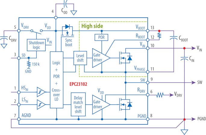
Figure 3. Functional block diagram of EPC23102. Image used courtesy of Bodo’s Power Systems [PDF]
These GaN ICs are designed for the indirect time of flight where it is necessary to switch 15 A at greater than 100 MHz.
Enhanced Functions in GaN Integration
Examples of enhanced functions in GaN integration are EPC’s ePower Stage ICs, such as EPC23102 [6]. These ICs are configured as half bridges with integrated full-featured gate drivers that include a level shifter, power-on reset, crossover protection, and delay matching. A functional block diagram for the ePower Stage IC is shown in Figure 3. These ICs are designed for a wide range of applications from motor drives with frequencies in the 10s to 100s of kHz, to high-frequency DC-to-DC converters up to 3 MHz. With this range of frequency, the switching speed must be able to be controlled without impacting the core gate drive performance.
One of the key advantages of GaN integration is that N-channel FETs are used in the output stage of the gate driver. Using an N-channel FET to drive the turn-on of the power FET allows resistor control of the turn-on to control the switching slew rate and thus overshoot and ringing. This is an important factor in controlling EMI and can be implemented without impacting other characteristics of the gate driver. A functional block diagram of an integrated power FET with a gate driver is shown in Figure 4 (a).
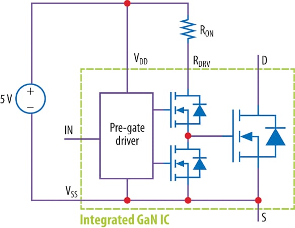
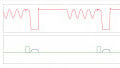
a. Image used courtesy of Bodo’s Power Systems [PDF]
b.
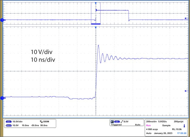
Figure 4. (a) Functional block diagram of GaN integrated power stage, (b) Switch node turn on of EPC9177 with 48 V in, 10 A out with ROn = 2.2 Ω. Image used courtesy of Bodo’s Power Systems [PDF]
EPC9177 [7] is an open-loop, half-bridge development board that uses EPC23102. With 2.2 Ω for ROn, at 48 V, 10 A, the turn-on switch node waveform is very well controlled as shown in Figure 4(b). Reduction of switch node ringing is critical for controlling EMI.
GaN Integration Conclusions
GaN integration provides numerous system benefits for many high-frequency applications. Integration reduces gate drive inductance and common source inductance, delivering fast current commutation speed. It allows tuning of commutation to reduce overshoot and ringing in the switch node, which is critical for EMI control. It reduces system size and cost by reducing component size and enabling increased frequency. GaN Integration reduces component count, reducing system cost and size while decreasing supply chain costs. GaN integration is just beginning, and the benefits are assured to increase over time.
References
[1] Lidow, Alex, de Rooij, Michael, Strydon, Johan, Reusch, David and Glaser, John, GaN Transistors for Efficient Power Conversion, Third Edition, John Wiley & Sons Ltd, 2020, pp 2-5.
[2] Lidow, Alex, GaN Power Devices and Applications, chapter 1, Efficient Power Conversion Corporation, 2022, p 16.
[3] Lidow, Alex and Strydom, Johan, eGaN® FET Drivers and Layout Considerations, https://epc-co.com/epc/Portals/0/epc/ documents/papers/eGaN%20FET%20Drivers%20and%20Layout%20Considerations.pdf, 2016.
[4] Lidow, Alex, de Rooij, Michael, Strydon, Johan, Reusch, David and Glaser, John, GaN Transistors for Efficient Power Conversion, Third Edition, John Wiley & Sons Ltd, 2020, pp 41 - 54.
[5] EPC2088 datasheet - https://epc-co.com/epc/Portals/0/epc/ documents/datasheets/EPC2088_datasheet.pdf, 2022.
[6] EPC23102 datasheet - https://epc-co.com/epc/Portals/0/epc/ documents/datasheets/EPC23102_datasheet.pdf, 2023.
[7] EPC9177 development board quick start guide - https://epc-co. com/epc/Portals/0/epc/documents/guides/EPC9177_qsg.pdf, 2023.
This article originally appeared in Bodo’s Power Systems [PDF] magazine
Featured image used courtesy of Adobe Stock