Facebook
 Google
 GitHub
 Linkedin
SemiQ Unwraps 1200 V SiC Modules Boasting Conversion Efficiency
At APEC 2026, SemiQ released a new family of high-performance half-bridge MOSFET modules to optimize power conversion for high-voltage applications.
SemiQ announced its QSiC Dual3 family at APEC 2026 in San Antonio. This series of 1200 V silicon carbide (SiC) half-bridge MOSFET modules is designed for high-voltage applications, including liquid-cooled data centers and industrial motor drives. At the conference, EEPower sat down with Jianfu Fu, SiC Module Application & Field Application Engineer, and Brian Patterson, Electrical Engineer, to learn more about these new products.
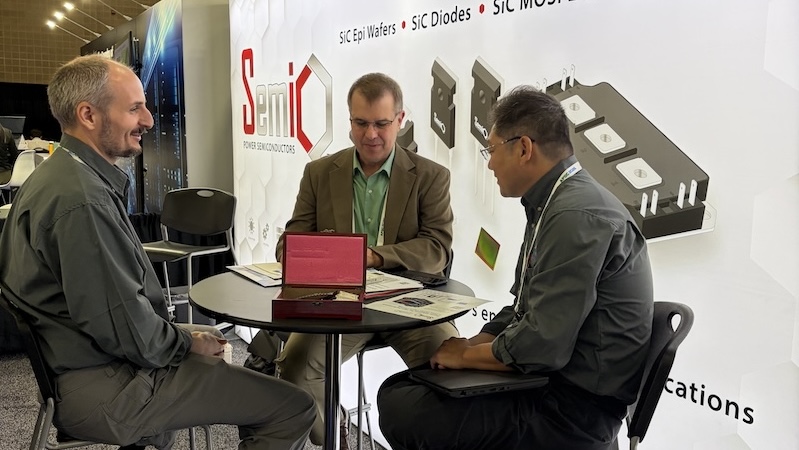
SemiQ's Brian Patterson (left) and Jianfu Fu (right) explained their new QSic Dual3 products to EEPower's Dale Wilson at APEC 2026.
The release comprises six distinct modules, each highlighting low on-resistance as its primary benefit, with the goal of maximizing conversion efficiency and power density in high-power industrial applications. According to Fu, these new modules incorporate the 3rd generation of the company's SiC technology. The die shrink allows them to fit more die into each module, thereby reducing RDS(on) and improving efficiency. Fu and Patterson went on to explain that everything inside the module must be symmetric, and that each die must be well matched.
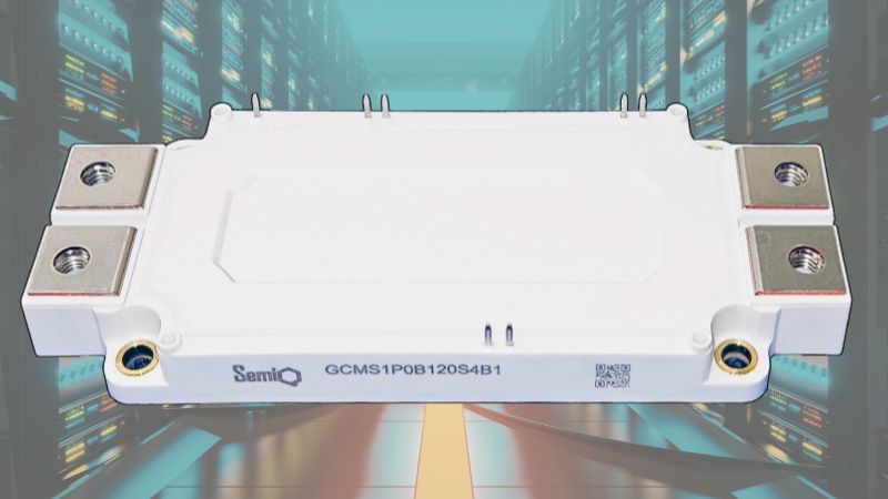
The QSiC Dual3. Image used courtesy of SemiQ
1200 V QSiC Dual3 Modules
At the highest level, the QSiC Dual3 modules are meant for efficient performance in harsh conditions.
A notable feature of the series is its power density, which reaches 240 W/in^3 in a 62 x 152 mm footprint. This is made possible by the series’ range of low-drain-source on-resistance options, including 1.0, 1.4, and 2.0 mΩ configurations.
For reliability purposes, SemiQ exposes each die to wafer-level gate-oxide burn-in tests at 1,450 V or higher during production. According to Fu and Patterson, this rigorous screening process, combined with a maximum junction temperature of 175°C, helps the modules to handle demanding power cycles common in heavy-duty industrial and data center applications.
Overview of the QSiC Dual3 modules. Video used courtesy of SemiQ
To achieve even greater thermal performance, SemiQ offers designers a ZTA-isolated baseplate that reduces junction-to-case thermal resistance. At the same time, a dedicated Kelvin reference pin provides a stable gate-source voltage control path, reducing source inductance.
The series offers these features in configurations both with and without integrated parallel SiC Schottky barrier diodes (SBD). For example, the GCMS1P0B120S4B1 model uses SBDs to eliminate reverse recovery losses, whereas the GCMX1P0B120S4B1 variant provides a standard MOSFET-only half-bridge.
Ultimately, SemiQ has positioned its module so that designers can replace existing IGBT designs with minimal redesign.
Understanding Reverse Recovery in Power Semiconductors
Reverse recovery is a phenomenon that occurs when a MOSFET’s body diode transitions from forward to reverse bias. During the forward-conduction phase, charge carriers accumulate in the semiconductor's drift region.
When the circuit applies a reverse voltage to turn the device off, these stored carriers do not disappear instantly. Instead, they must be swept out or recombined before the device can successfully block the reverse voltage. This process creates a transient reverse current, known as the reverse recovery current, which flows in the opposite direction of the initial forward current.
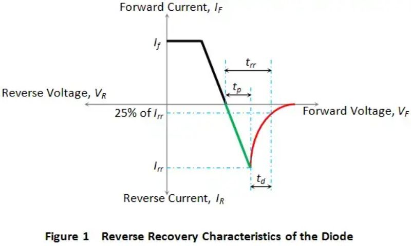
Reverse recovery time of the diode. Image used courtesy of PCB Hero
The energy lost during this transition directly contributes to switching losses in a power converter. As switching frequencies increase to reduce the size of passive components like inductors and capacitors, these losses become more significant, leading to higher heat generation and reduced system efficiency.
In silicon-based PiN diodes, reverse recovery is highly dependent on temperature and the rate of current change, often requiring larger heatsinks to manage the resulting thermal load. Silicon carbide Schottky barrier diodes address this challenge because they are unipolar devices that do not store minority carriers in a drift region.
Consequently, they exhibit near-zero reverse recovery current and independent temperature characteristics, allowing for more efficient high-speed switching.
Future Potential for High-Density Power Conversion
SemiQ’s QSiC Dual3 modules could offer a path for designers to create smaller, lighter power conversion systems. By reducing overall energy loss during conversion, these modules can help operators lower the total cost of ownership for large-scale infrastructure. Interestingly, will most companies at APEC 2026 were focused on the power inside the AI data center racks, SemiQ is targeting other high-power applications in the centers, including the power chiller used to provide cooling to the entire building.