 Facebook
 Google
 GitHub
 Linkedin
Renesas Adds High- and Low-Voltage GaN Devices for AI Data Centers
The 650 V dual-side-cooled FET cuts footprint by 57% versus TOLT, while its 100V E-mode family delivers 40-70% lower switching losses and 1-3% higher efficiency than silicon.
Renesas has introduced two GaN devices designed for AI data centers and industrial applications. The first is the TP65H020G4PLSGBD: a 650 V GaN FET rated at 20 mΩ, housed in a dual-side-cooled 8x8 mm PQFN and aimed at the intermediate bus, battery backup, and capacitor bank stages of 800V AI data center racks.
The second development is the RTP100 series: four 100 V E-mode transistors from 5 mΩ to 1.2 mΩ, aimed at synchronous rectification and multiphase buck stages in AI servers, robotics, and industrial motor drives.
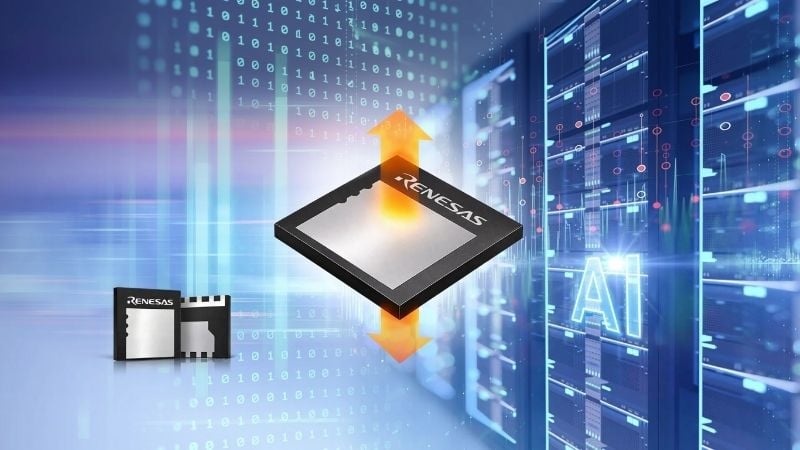
The TP65H020G4PLSGBD dissipates heat through both package faces. Image used courtesy of Renesas
Dual-Side Cooling Buys Back Board Space at 650V
The high-voltage part is the TP65H020G4PLSGBD, a 650 V, 20 mΩ SuperGaN FET on Renesas’ Gen IV Plus platform, rated at 92 A continuous at 25°C. Renesas says it is the first 650 V GaN device to use dual-side cooling, which lets it fit in an 8x8 mm PQFN.
That package is the point. Conventional top-side-cooled parts move heat through a single face, so the outline has to stay physically large enough to sustain that one thermal path—a floor set by cooling, not by the die. Pulling heat through both faces relaxes it.
The outline drops from 10x15 mm TOLT to 8x8 mm, a 57% reduction in area, while lowering top-side thermal impedance by 10%. For racks climbing from roughly 120 kW toward the megawatt scale, the binding constraint is physical before it is electrical: the board runs out of room, and the heatsink runs out of margin while the silicon still has more to give.
The internal structure explains the drive story. The part pairs a depletion-mode GaN HEMT with a low-voltage silicon MOSFET, making the switch normally off and letting a standard silicon driver handle it—no negative bias, no E-mode-specific drive circuitry, and a drive stage that carries over from an existing silicon design.
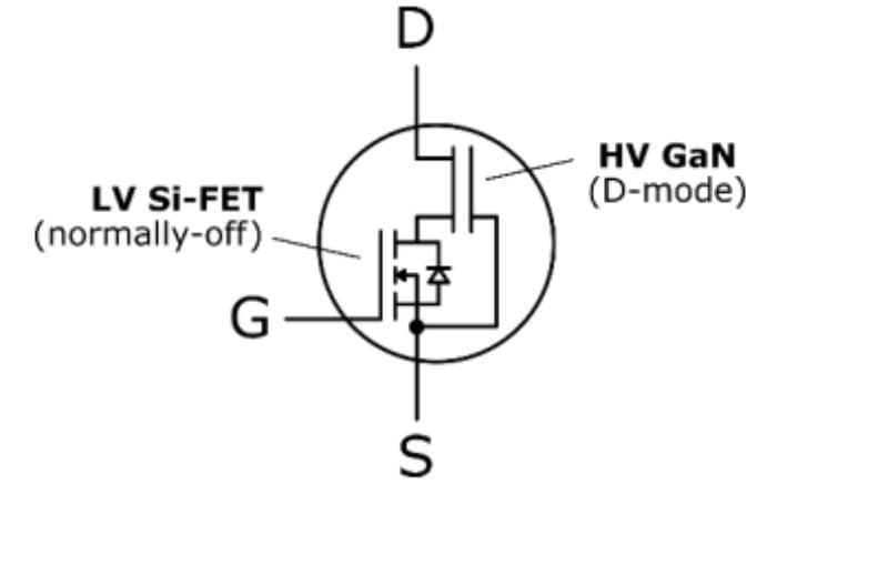
Block diagram of the TP65H020G4PLSGBD. Image used courtesy of Renesas
A high threshold voltage, negligible reverse recovery, and low gate and output charge let the part switch into the megahertz range, shrinking the magnetics and filtering that dominate converter volume.
Renesas has silicon to back it. A 6 kW 800 V-to-48 V LLC DC transformer built on the part, controlled by an RA6T3 MCU, reaches 2.6 kW/in³, with per-module testing measuring full-load efficiency 0.21% above an equivalent TOLT board.
The device is sampling now, with mass production scheduled for mid-2027.
Four Parts, One Silicon-Compatible Footprint at 100V
The low-voltage side is a family of four 100 V E-mode GaN transistors built on Renesas’ Gen 1 RexGaN platform: the RTP100E005G1FL at 5 mΩ and RTP100E2P6G1FL at 2.6 mΩ in bottom-cooled packages, and the RTP100E1P8G1FL-DSC at 1.8 mΩ and RTP100E1P2G1FL-DSC at 1.2 mΩ with dual-side cooling. These are the company’s first low-voltage GaN parts.

The low-voltage GaN FETs target humanoid robotics, factory automation, and AI data centers. Image used courtesy of Renesas
While the 650 V device reaches silicon compatibility through its internal structure, this family achieves it natively. E-mode GaN is normally off by design, and the parts use footprints matched to their silicon counterparts, so a designer migrating from a silicon layout can keep both the drive scheme and, largely, the board.
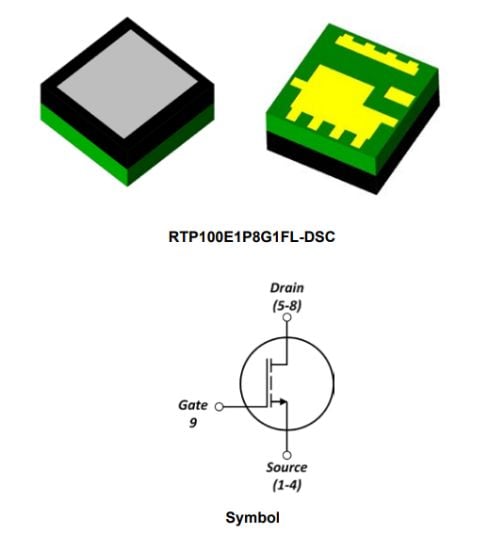
The dual-side-cooled RTP100E1P8G1FL-DSC. Image used courtesy of Renesas
The gains come from how little charge the devices move. Every switching transition costs energy to charge and discharge the gate and the output node, and that cost repeats every cycle, so at megahertz rates it dominates. Keeping both charges low makes each transition cheaper.
The datasheet also specifies zero reverse recovery, removing a loss that silicon pays on every hard-switched turn-on. The combined effect is 40 to 70% lower switching losses and 1 to 3% higher efficiency than silicon designs.
Those numbers matter because of where converter design is heading. Data center power stages have generally run at a few hundred kilohertz; as racks move to 800 V distribution and 48 V buses, more of those stages are pushing toward megahertz switching. Frequency shrinks magnetics, and magnetics set converter volume. The company claims up to double the system power density, with smaller fans and less active cooling as a second-order effect.
The family is not data center exclusive. Renesas targets synchronous rectification and multiphase buck stages in markets ranging from AI servers and robotics to factory automation, power tools, and solar microinverters.
All four are available now, with evaluation boards.
What Comes Next
The two launches reach customers on very different schedules. The low-voltage parts ship today with evaluation boards; the 650 V device is sampling, with volume production set for mid-2027. That gap tracks the architectures themselves; 48V designs are in production now, while 800 V racks are still being specified.