Facebook
 Google
 GitHub
 Linkedin
Low Voltage GaN Surpasses MOSFETs in AI Power Density
AI workloads are reshaping computing server power delivery requirements. Low-voltage GaN is emerging as a key enabler of higher efficiency and greater power density than silicon MOSFETs in next-generation AI infrastructure.
Article co-authored by EPC’s Alejandro Pozo and Michael De Rooij.
This article is published by EEPower as part of an exclusive digital content partnership with Bodo’s Power Systems.
Artificial intelligence is integrating into our professional and personal lives at an unprecedented pace. By streamlining software development, tackling complex analytical challenges, and automating routine documentation, AI is no longer just a tool; it’s a fundamental shift in how we create and solve.
These new-generation AI servers come at a cost based in large part on an exponentially increasing demand for power. The center of this power consumption is the Graphics Processing Unit (GPU) made from billions of microscopic transistors compacted on a silicon substrate with features as small as 20 Å (That’s approximately the width of the DNA molecule’s double helix). The power required to activate these billions of processing agents is going up as fast as their computational capabilities. Table 1 shows an example that uses Nvidia’s published roadmap through 2028.
Table 1. Power Requirements for AI GPUs [1,2].
| Architecture | Year | Typical GPU TDP | Cooling Method |
| Blackwell | 2024 | 1,000 W – 1,400 W | Air / Liquid |
| Rubin | 2026 | 2,300 W – 3,600 W | Liquid (Mandatory) |
| Feynman | 2028 | 4,400 W – 6,000 W | Immersion / Embedded |
The NVIDIA Vera Rubin architecture typically features two Rubin GPUs on a single server board. These are paired with one Vera CPU to form what is known as the Vera Rubin Superchip. Each board requires as much as 12 kW delivered to all the various elements, in addition to the Superchip. A standard NVIDIA Vera Rubin NVL72 server rack typically contains 18 server boards for a total requirement of 216 kW per rack.
By the time Feynman is released, that number at least doubles, with a 1 MW rack not too far in the future.
Delivering the Power Within the Rack
Distributing 216 kW within a rack is not easy. Today, the rack is provided with 3-phase 415 VAC, delivered with a neutral so that individual power supplies within the rack can be powered from 240 VAC each. Internally, each power supply converts the 240 VAC to 400 VDC, and then further to 48 VDC while providing safety isolation. All this resides in power trays co-located inside the data server rack. The 48 VDC is then distributed to each server tray, where the electrons proceed to be processed down to less than 1 VDC.
The Blackwell generation server board requires up to 3 kW. That is 62.5 A going to the server board from the power supply in the rack. However, for a Rubin system at 12 kW, the current increases to 250 A, which is quite difficult to handle through commonly available connectors and bussing. Now triple that number for the Feynman generation, and the amount of current becomes impractical to deliver through the connectors to the board.
The inevitable solution involves higher voltages delivered to the server board and distribution within the rack. The prevailing thought is that this new voltage will be either 800 V or +/- 400 V. In either case, the current flowing to the board is reduced to 15 A for a typical Vera Rubin server board.
Three different power delivery architectures are shown in Figure 1. The distribution voltage of either +/- 400 V or 800 V comes from a separate designated power rack called a “sidecar”. In the lower two cases, the high voltage is bussed to the server board directly, where it is converted to either 6 VDC or 12 VDC. Both voltages are planned by different server manufacturers. The last case shown at the top of Figure 1 maintains the more traditional configuration where the 800 V is converted to 48 VDC.
There are two scenarios for this approach, where the first maintains the traditional power shelf with 48 V distribution, taking advantage of the higher power density of the power supply, but would require much thicker power bussing throughout the rack. The second approach uses a compact 800 V to 48 V converter locally at each server board, but this occupies precious area needed for the processor. Overall, these 48 V approaches maintain utilization of traditional hardware on the server board, thus easing the transition to higher power levels as the server rack design evolves.
The server board is considered precious real estate, and therefore the power delivery needs to take up as little space as possible while maintaining extreme conversion efficiency. Any power converter on the server card would need not only to occupy the least amount of space but also to be extremely thin to accommodate the tight board-to-board spacing as well as the aggressive thermal management systems (see Table 1) that would be deployed throughout the board.
One solution that demonstrates the highest efficiency, highest power density, and thinnest form factor is the ISOP converter (Inputs in Series, Outputs in Parallel) [3,4]. The basic ISOP configuration, shown in Figure 2, uses low-voltage devices in a stacked series of LLC converters with their outputs connected in parallel. An ISOP operating from 800 V can be realized using 8 modules configured with 150 V-rated GaN FETs [5], instead of 650 V-rated devices as would be used in a two-stage converter.
Lower voltage devices yield much lower conduction losses and have a higher effective operating duty cycle, thus reducing ripple current losses compared to higher voltage counterparts. In addition, the higher number of stages allows for better thermal distribution and lower output ripple current when the LLC module operation is interleaved. There are also EMI benefits to using a higher number of modules in the ISOP configuration due to the reduced voltage of the high dv/dt transitions, as shown in Figure 3.
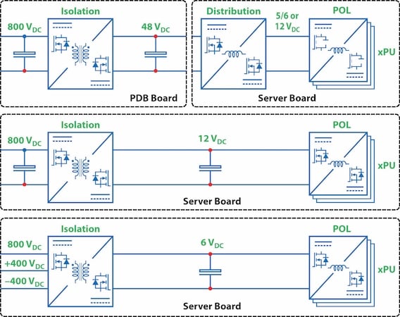
Figure 1. Three different power delivery architectures under consideration for the next generations of AI servers. Image used courtesy of Bodo’s Power Systems [PDF]
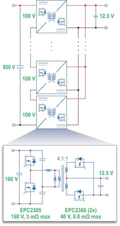
Figure 2. The basic ISOP concept is to use low-voltage devices in a stacked series of LLC converters with their outputs connected in parallel. Image used courtesy of Bodo’s Power Systems [PDF]
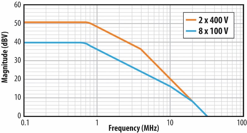
Figure 3. Difference in E-field generation between a two-stage ISOP with a 400 V bus and an eight-stage ISOP with a 100 V bus for a system operating at 800 V and switching at 1 MHz. Image used courtesy of Bodo’s Power Systems [PDF]
Figure 4 is an example of a 6 kW ISOP converter that has an input voltage of 800 VDC and an unregulated output voltage of 12.5 VDC. The conversion efficiency at full load is 97%, and the entire converter occupies less than 5,000 mm2 with a thickness of just 8 mm. A similar ISOP approach can yield a thin, small, and efficient 800 VDC to 6 VDC on-board converter.
The choice between distributing the voltage on the server board at 12 V or 6 V is a challenging trade-off between distribution losses and conversion losses. At 12 V, the losses on the server board are four times less for the same amount of copper routing. A 6 V bus can be more easily and efficiently converted using a single stage to sub-one-volt level, especially considering the newest generation GaN transistors made for lower voltage conversion, but the higher losses throughout the server board may compensate.
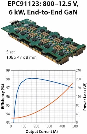
Figure 4. The EPC91123 is an 800 VDC – 12.5 VDC, 6 kW, eight-stage ISOP DCDC converter that is only 8 mm thick and is designed to be mounted directly on the server board. This converter has a peak efficiency of 98.3% and a full-load efficiency of 97%. Image used courtesy of Bodo’s Power Systems [PDF]
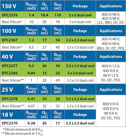
Table 2. The latest generation GaN transistors have lower RDS(on) and better switching characteristics than the best-in-class (BiC) silicon MOSFETs. Image used courtesy of Bodo’s Power Systems [PDF]
Unseating the Aging MOSFET in AI Servers:
Power MOSFETs have been an essential component in power conversion for almost 50 years, while GaN transistors have been in mass production for over 16 years [6]. GaN devices hold the promise of being far smaller and more efficient than silicon MOSFETs, yet, until recently, that promise has only been a reality for devices with voltage ratings between 100 V and 650 V.
Recent advances in GaN technology made by Efficient Power Conversion, have resulted in a whole new generation of GaN transistors that outperform silicon MOSFETs in size, efficiency, and speed for voltage ratings all the way down to 15 V and less. Table 2 is the evidence. In this table, benchmark GaN devices are shown from 150 V down to 15 V, compared with the benchmark MOSFET in the same, or, in some cases, larger-footprint packages.
For applications such as power-hungry, space-sensitive AI servers, there is no reason to choose aging silicon MOSFETs over the latest-generation GaN devices. In addition, GaN is still a relatively young technology, and there are many improvements coming in the next few years that will only make the GaN-silicon gap even wider.
Conclusions
This article presented the shift in server power architectures brought about by artificial intelligence and explained how GaN FETs provide the solutions to meet the ever-increasing power density demands. A 6 kW 800 V to 12.5 V input series output parallel converter using low voltage GaN FETs yields power densities exceeding 1.2 W/mm2 and a full load efficiency of 97%, which was given as an example of GaN FET capability. Newer low-voltage devices with extremely low on-resistance and gate charge further open the door for GaN FETs to become the new device of choice in point-of-load conversion.
References
[1] W. Chu, D. Patel, D. Nishball, et al, “Vera Rubin – Extreme Co Design: An Evolution from Grace Blackwell Oberon” Semianalysis newsletter, February 25, 2026
[2] A. Shilov, “Future AI processors said to consume up to 15,360 watts of power — massive power draw will demand exotic immersion and embedded cooling tech”
[3] A. Pozo and S. Colino, “Low Cost and Low Profile 800 VDC to 12.5 V DC-DC Converter Using Low Voltage GaN in an ISOP Topology,” Efficient Power Conversion white paper.
[4] Q. Ma, Q. Huang and A. Q. Huang, “Zero-Voltage Switching and Natural Voltage Balancing of a 3 kW 1 MHz Input-SeriesOutput-Parallel GaN LLC Converter,” in IEEE Open Journal of Power Electronics, vol. 5, pp. 1119-1128, 2024, doi: 10.1109/ OJPEL.2024.3433562.
[5] Efficient Power conversion, “EPC2305 – Enhancement Mode Transistor”
[6] A. Lidow, M. de Rooij, J. Glaser, A. Pozo, S. Zhang, M. Palma, D. Reusch, and J. Strydom, “GaN Transistors for Efficient Power Conversion”, 4th ed. John Wiley & Sons, 2025. ISBN: 978-1394286959
This article originally appeared in Bodo’s Power Systems [PDF] magazine and is co-authored by Alex Lidow, CEO; Alejandro Pozo, Director of Applications Engineering; and Michael De Rooij, GaN Applications Fellow, Efficient Power Conversion (EPC)