Facebook
 Google
 GitHub
 Linkedin
Navitas Skips 48 V Bus in 800 V-to-6 V GaN PDB for AI Racks
GaN-based power delivery board targets 96.5% efficiency and 2,100 W/in3 for NVIDIA's next-generation 800 VDC data center architecture.
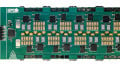
Navitas Semiconductor unveiled a DC-DC power delivery board (PDB) at Nvidia GTC 2026 in San Jose that converts 800 V directly to 6 V in a single power stage, eliminating the traditional 48 V intermediate bus converter (IBC) entirely.
The board, built on Navitas' GaNFast gallium nitride technology, targets up to 96.5% peak efficiency at full load with a 1 MHz switching frequency and a power density of 2,100 watts per cubic inch (W/in3). The PDB is designed for NVIDIA's emerging 800 VDC data center power architecture, which replaces legacy 54 V in-rack distribution to support megawatt-class AI rack densities that older power delivery chains cannot sustain.
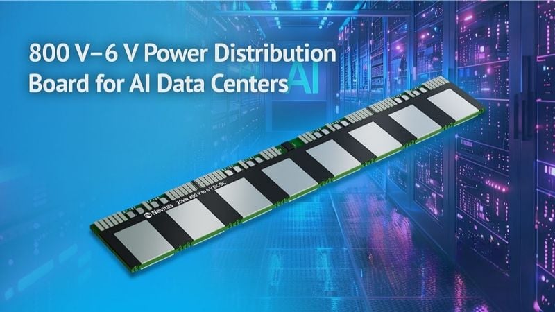
800 V-6 VDC-DC power delivery board. Image used courtesy of Navitas
Why Skip the Intermediate Bus
Traditional enterprise and cloud server architectures distribute power at 54 V inside the rack. Power supply units convert AC mains to 54 V, then an intermediate bus converter steps that down to 12 V or lower for the voltage regulator modules feeding GPUs and CPUs.
As rack power scales toward 1 MW for platforms like Nvidia’s Kyber, which will house 576 Rubin Ultra GPUs by 2027, that 54 V distribution model hits hard physical limits. Powering a single 1 MW rack at 54 VDC would require up to 200 kg of copper busbar, and the repeated AC-DC and DC-DC conversion stages accumulate losses at every step.
Nvidia’s solution is to distribute 800 VDC from centralized rectifiers directly to each compute node, with this higher voltage dramatically reducing current and copper requirements. Over 150% more power can be transmitted through the same copper at 800 VDC compared to traditional architectures.
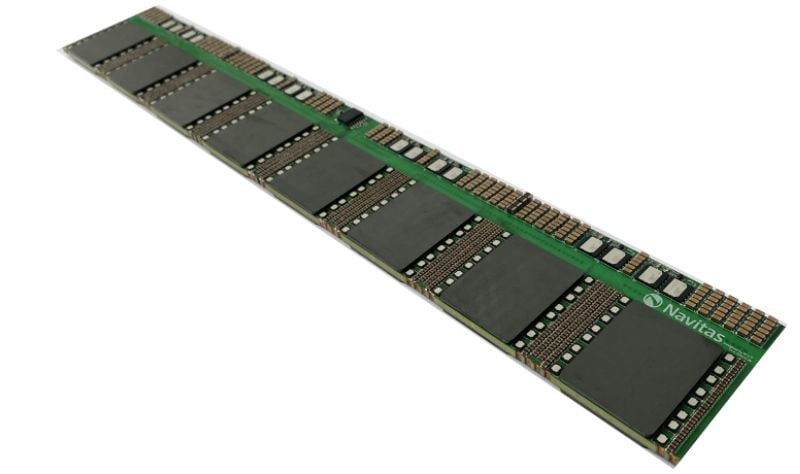
The 800 V-6 V DC-DC PDB. Image used courtesy of Navitas
Navitas had previously released an 800 V-to-50 V platform, but that still required a downstream VRM stage to reach the sub-12 V levels that processors need. The new 800 V-to-6 V board removes that intermediate step completely. By outputting 6 V instead of the 12 V used in competing designs, Navitas stated that the VRM conversion ratio is cut in half, reducing losses in that final power stage as well.
What’s Inside the Board
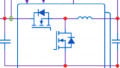
The primary side uses 16 x 650 V GaNFast FETs in Navitas' latest DFN8x8 dual-cooled package, arranged in a stacked full-bridge configuration. The secondary side uses center-tapped outputs with 25 V silicon MOSFETs. Switching at 1 MHz allows the use of the smallest passive components and planar magnetics, which is how the board achieves its 2,100 W/in3 density.
The board's profile is approximately 20% thinner than a mobile phone, allowing it to sit close to the GPU board for tighter power loop integration and improved transient response. That physical proximity is key because shorter power traces between the PDB and the processor reduce parasitic inductance and resistive losses.
A Crowded Race
Navitas is not the only GaN vendor targeting the 800 VDC transition. Infineon has also launched two CoolGaN-based high-voltage IBC reference designs: an 800 V-to-50 V design that demonstrated over 98% efficiency at full load with a power density of 2.5 kW/in3, while its 800 V-to-12 V design achieved 98.2% peak efficiency and a power density exceeding 2,300 W/in3 in a form factor just 8 mm tall.
The two companies are taking different architectural approaches, with Infineon's designs retaining the intermediate bus, stepping down to 50 V or 12 V before a final VRM stage handles the last conversion. Navitas is attempting to collapse that chain into a single step all the way to 6 V. There’s a trade-off between complexity on the primary side and efficiency across the full delivery path.
Nvidia’s 800 VDC silicon ecosystem now includes over a dozen partners, among them Analog Devices, EPC, Infineon, Innoscience, MPS, Navitas, onsemi, Power Integrations, Renesas, ROHM, STMicroelectronics, and Texas Instruments. Kyber racks are not expected to ship until 2027, giving the supply chain time to settle on which conversion strategies deliver the best balance of efficiency, density, and cost at scale.
Related Content