Facebook
 Google
 GitHub
 Linkedin
Alpha and Omega Debuts 600 V Super Junction MOSFETs
AOS pairs its aMOS E2 high-voltage MOSFET platform with the top-side cooled GTPAK package, targeting power supplies, solar inverters, and industrial systems.
Alpha and Omega Semiconductor (AOS) has released two 600 V super junction MOSFETs built on its newly developed aMOS E2 high-voltage platform. The AOGT037V60DE2 and AOGT060V60DE2 combine low on-resistance with AOS's proprietary top-side cooled GTPAK package, offering power designers a path to higher density and improved thermal management in AC-DC, DC-DC, and DC-AC converter designs.
Both devices are now available in production quantities, with the Sunnyvale, California-based company positioning the platform as an answer to the thermal and EMI constraints that have long plagued traditional bottom-cooled high-voltage MOSFETs.
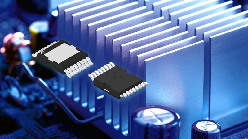
The αMOS E2 600 V Super Junction MOSFETs. Image used courtesy of AOS
Top-Side Cooling Meets Super Junction Silicon
The aMOS E2 platform was engineered to address two persistent challenges in high-voltage power design: thermal extraction and electromagnetic interference. Traditional bottom-side-cooled packages force designers to route heat through the PCB, constraining board layout and limiting achievable power density in a given form factor. AOS's GTPAK package flips that arrangement by placing the cooling pad on top, allowing direct heatsink attachment and freeing up PCB real estate underneath for other components or tighter routing.
The AOGT037V60DE2 offers 37 milliohms of on-resistance, while the AOGT060V60DE2 offers 60 milliohms. Both are rated for 600 V and feature gull-wing leads, which AOS said improve board-level reliability in mission-critical environments subject to vibration and thermal cycling.
The package co-optimizes the electrical and thermal paths, meaning system designers can extract maximum performance from the silicon without the layout compromises that bottom-cooled alternatives typically impose.
Beyond the package, the aMOS E2 silicon itself includes several ruggedness features for industrial and renewable energy applications. Body-diode ruggedness is rated at 1500 A/us, and the devices offer superior avalanche capability alongside short-circuit withstand time. A built-in fast body diode reduces reverse recovery charge, which is particularly valuable in hard-switching topologies and totem-pole PFC circuits where diode recovery losses can significantly erode system efficiency.
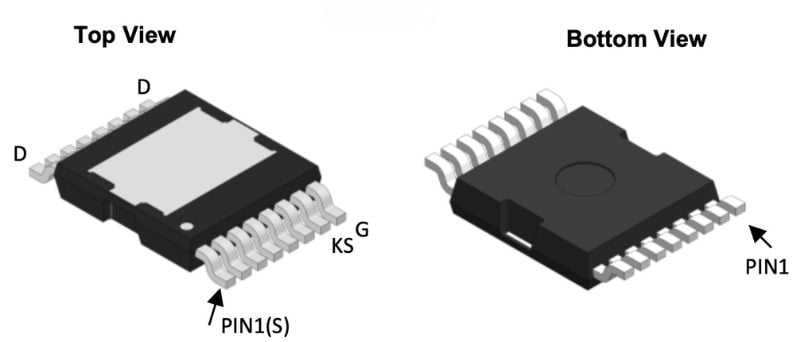
The GTPAK. Image used courtesy of AOS
AOS also highlights the platform's resistance to self-turn-on under dynamic switching conditions, along with strong inrush current handling and wide safe operating area capabilities.
Broad Topology Support Across Power Applications
AOS is targeting the aMOS E2 GTPAK devices at a wide range of higher-voltage power conversion topologies. These include boost PFC, totem-pole PFC slow-leg operation, LLC resonant converters, phase-shifted full bridge, cyclo-converters, and CrCM H-4/cyclo inverter designs. The application scope spans servers, workstations, telecom rectifiers, solar inverters, motor drives, and industrial power systems.
Combining top-side cooling and robust super junction silicon is particularly relevant in renewable energy and telecom infrastructure, where converters must sustain high power throughput while meeting increasingly strict thermal and EMC requirements. By reclaiming the PCB area a traditional bottom-cooled package would occupy, the GTPAK lets engineers shrink the overall power stage or add functionality without increasing board size.
In totem-pole PFC designs, for instance, the slow-leg MOSFET must handle significant reverse recovery stress from its body diode. The aMOS E2's 1500 A/us di/dt rating and reduced reverse recovery charge directly address that requirement, potentially letting designers avoid external diode networks or snubber circuits that lower-ruggedness MOSFETs would demand.
Similarly, in LLC resonant converters, the combination of low on-resistance and controlled output capacitance characteristics influences the resonant tank's behavior and overall conversion efficiency.