Facebook
 Google
 GitHub
 Linkedin
Inside the Silicon Carbide JFET: Specs, Stability, and the New Performance Frontier
Learn how SiC JFETs beat MOSFETs for next-gen power. They offer ultralow loss, superior stability, and rugged avalanche protection—critical for high-voltage solid-state power distribution.
Article co-authored by Infineon’s Elijah Fagbemi.
This article is published by EEPower as part of an exclusive digital content partnership with Bodo’s Power Systems.
JFETs have advantages over MOSFETs for specialized applications such as high-voltage SSCBs. Global electricity consumption continues to rise sharply across regions, sectors, and end‑use systems. Electrification of transport, heating and cooling, industrial equipment, and data center expansion are among the strongest contributors to this trend (IEA, 2025). As demand grows, so does the pressure on distribution infrastructure to operate faster, safer, and more efficiently.
Traditional electromechanical switching, designed for a different era, cannot meet the microsecond-scale response times and long-life reliability now expected. The shift toward solid-state architectures reflects this need for speed, precision, and durability.

Image used courtesy of Adobe Stock
As power systems evolve, so does the semiconductor technology enabling them. Widebandgap (WBG) materials, especially silicon carbide (SiC), have become foundational for high-voltage, high-current switching thanks to their thermal performance, low losses, and voltage-handling capability.
SiC MOSFETs are well-established, but recent advancements highlight another device class whose time has come again: the silicon carbide junction field-effect transistor (JFET). Fabrication maturity, improved packaging, and the emergence of high-voltage solid-state power distribution (HV SSPD) make the SiC JFET newly relevant and powerfully differentiated.
These system-level requirements have elevated the role of SiC, now the primary WBG material enabling (HV SSPD). In this context, SiC JFETs stand out for their ability to pair extremely low conduction losses with high robustness, making them a compelling fit for fault-tolerant, high-current distribution architectures.
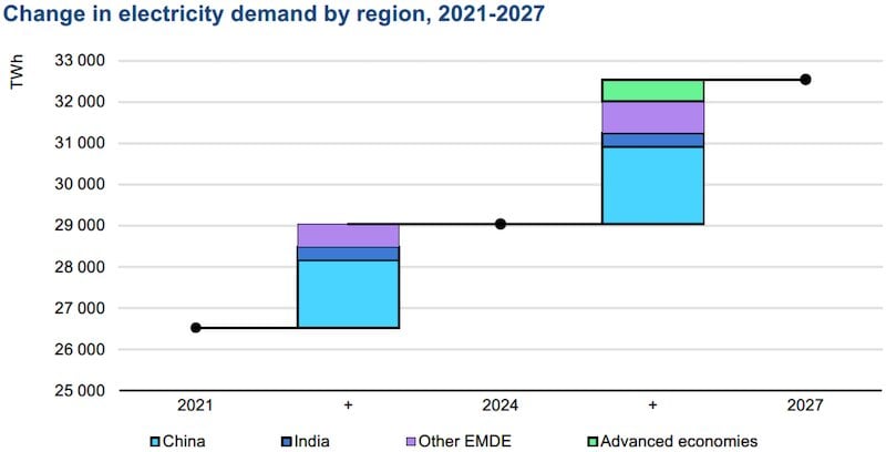
Figure 1. Change in electricity demand by region, 2021–2027. Note: EMDE = Emerging Markets and Developing Economies [1]. Image used courtesy of Bodo’s Power Systems [PDF]
Why the SiC JFET is Reemerging
Several industry trends have converged to lift the SiC JFET back into prominence.
1. SiC manufacturing has improved significantly, reducing variability and enabling larger die with consistent performance
2. Modern packaging - especially thermally optimized, topside-cooled designs - supports higher current densities
3. The rise of HV SSPD has created demand for devices with ultralow RDS(on), stable linearmode behavior, and high avalanche robustness
These characteristics are the JFET’s natural strengths. Devices now achieve best-in-class typical RDS(on) values such as 1.6 mΩ at 750 V and 2.3 mΩ at 1200 V. This makes them ideal for current-intensive applications where conduction loss dominates total system loss.
Device Construction and Operating Principles
Modern SiC JFETs typically use a trench-based structure with a p-type gate region sculpted into the n-type drift zone. This creates a vertical channel whose conductivity is modulated by gate voltage. The structure is optimized to minimize the RDS(on) × A figure-of-merit (FOM) while maintaining thermal stability and robust avalanche behavior.
During on-state conduction, current flows through the volume channel, while in the off-state, the space-charge region expands to pinch off conduction. Because the device is normally on, it provides extremely low resistance when conducting but requires careful control to ensure a safe turnoff. These characteristics can be managed either through gatedrive schemes or through cascode configurations where a low-voltage MOSFET controls the JFET gate indirectly.
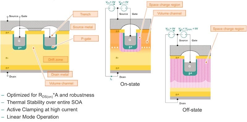
Figure 2. Cross‑section of trench‑based SiC JFET showing P‑gate, drift region, and channel. Image used courtesy of Bodo’s Power Systems [PDF]
Ultralow RDS(on): Scaling Efficiency and Density
In high-current distribution and protection systems, designing components to manage conduction loss becomes a dominant contributor to footprint, thermal design effort, and cost. SiC JFETs currently deliver some of the lowest device-level RDS(on) values available in their voltage classes, with typical ratings such as:
- 1.6 mΩ (750 V)
- 2.3 mΩ (1200 V)
This performance supports system designs operating at 32 A to 63 A and above, within compact footprints—levels that would require significantly larger silicon or MOSFET-based stages.
Lower conduction loss also reduces heatsink mass and cooling requirements, improving system compactness and lowering overall cost.
Improved Linearmode Stability for Safe Inrush Handling
A defining strength of the SiC JFET is its improvement in stability in linear mode, compared to a SiC MOSFET. When a system powers a capacitive load, the device can safely operate in a high-resistance regime, naturally limiting inrush current without additional circuitry.
This simplifies the implementation of “connect” functions such as precharging, hotswap operations, and soft starts. It also reduces stress on both the device and the surrounding system during high-current transients.
Avalanche Robustness for Inductive Disconnect
Disconnecting inductive loads can generate large overvoltage spikes. SiC JFETs are rated for; and productiontested in; highcurrent avalanche conditions, allowing them to clamp these events safely.
This high avalanche energy handling:
- Reduces the need for external clamping networks
- Improves current sharing during paralleling
- Enhances reliability during repeated inductive switching cycles
Some JFET-based implementations still need metal oxide varistors (MOVs) or transient voltage suppression (TVS), but they reduce the MOV + RC snubber combinations required by MOSFET architectures, reducing BOM complexity and potential failure points.
Packaging and System Integration: The Role of QDPAK
Packaging is crucial for realizing device potential. The QDPAK form factor used in CoolSiC™ JFETs incorporates:
- Large drain and source interface areas for low electrical resistance
- A large, topside-cooled heatslug for low Rth
- Internal diffusion soldering for high current capability
- Extendable thermal capacitance to adapt to overload behavior
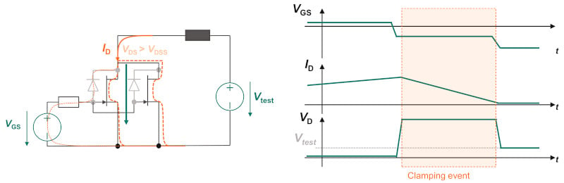
Figure 3. Overvoltage clamping waveform demonstrating stable avalanche behavior. Image used courtesy of Bodo’s Power Systems [PDF]
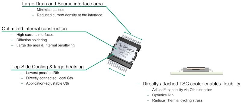
Figure 4. Q‑DPAK package layout illustrating drain/source pads and heatslug. Image used courtesy of Bodo’s Power Systems [PDF]
This approach directly supports high-current SSPD designs by minimizing temperature rise and reducing interface bottlenecks.
Driving Concepts: Normally ON and Cascode Options
Although the JFET is inherently normally on, several practical driving strategies exist:
- Direct drive with negative gate bias
- Classic cascode using a low-voltage MOSFET for normally off behavior
- Adapted cascode with additional gate network tuning
These options improve compatibility with existing MOSFET-oriented architectures, giving system designers flexibility to integrate JFETs without major architectural redesign.
JFET vs. MOSFET: A Comprehensive Comparison
Table 1. JFET vs. MOSFET comparison across critical dimensions
| Dimension | SiC MOSFET | SiC JFET |
| Conduction mechanism | Channel conduction | Bulk conduction |
| Gate structure | Fully isolated | Non‑isolated p‑gate |
| Normal state | Normally off | Normally on |
| RDS(on) | Higher for the same voltage class | Lowest per device |
| Temperature coefficient | Lower | Higher but stable SOA |
| Linear‑mode capability | Limited | Improved, inrush‑limiting |
| Avalanche behavior | Good, but requires clamping | Highly rugged, simplifies clamping |
| Control complexity | Simple | Requires a drive strategy or cascode |
| System implications | Best for legacy‑friendly designs | Best for maximum power density and protection |
Business Implications
While technical differentiation matters, evaluating SiC device choices focuses on system‑level outcomes. Several implications stand out:
- Lower TCO from miniaturization and reduced cooling requirements
- Simplified architecture from reduced clamping components and fewer failure modes
- Higher reliability through stable linear ‑mode operation and robust avalanche capability
- Scalability in improved thermal performance using advanced packaging like Q‑DPAK
These advantages translate directly into operational efficiency, long‑life performance, and reduced downtime for critical infrastructure.
Conclusion
The SiC JFET has returned to prominence not because it replaces MOSFETs, but because it excels in domains where ultralow conduction loss, linear‑mode stability, and avalanche resilience are essential. Today’s power‑distribution landscape demands precisely these characteristics, particularly as systems evolve toward solid‑state protection, compact power stages, and long‑lifetime operation.
With manufacturing improvements, advanced packaging, and flexible control strategies, modern SiC JFETs present a compelling option for high-current, high-reliability designs. For businesses rethinking their next-generation power architectures, exploring what CoolSiC™ JFETs can offer is a strategic step toward meeting the demands of an increasingly electrified world.
To learn more about the CoolSiC™ JFET family, visit:
https://www.infineon.com/product-information/power/silicon-carbide-jfets
This article originally appeared in Bodo’s Power Systems [PDF] magazine and is co-authored by Rene Mente, Principal Engineer, Technical Marketing, and Elijah Fagbemi, Product Marketing Manager, both for HV MOSFETs, Infineon Technologies