 Facebook
 Google
 GitHub
 Linkedin
Why a Stable Switch-Mode Power Supply May Still Oscillate
A perfectly stable switch-mode power supply may still oscillate due to its negative resistance at the input. This article examines the issue using LTspice.
This article is published by EE Power as part of an exclusive digital content partnership with Bodo’s Power Systems.
A perfectly stable switch-mode power supply (SMPS) may still oscillate due to its negative resistance at the input. The SMPS looks like a small signal negative resistance at the input. With input inductance and capacitance, it may form an undamped oscillation circuit.
Switch-Mode Regulators
The function of a switch-mode regulator is to convert the input voltage to a regulated constant output voltage as efficiently as possible.

Image used courtesy of Adobe Stock
There are some losses to this process, and the efficiency is measured as
\[\eta=\frac{P_{OUT}}{P_{IN}}\longleftrightarrow P_{IN}=\frac{P_{OUT}}{\eta}\rightarrow V_{IN}\times I_{IN} =\,\,\,\,\,\,\,\,\,\,\,\,\,\,(1)\\ \frac{V_{OUT}\times I_{OUT}}{\eta}\longleftrightarrow I_{IN}=\frac{V_{OUT}\times I_{OUT}}{\eta}/V_{IN}\]
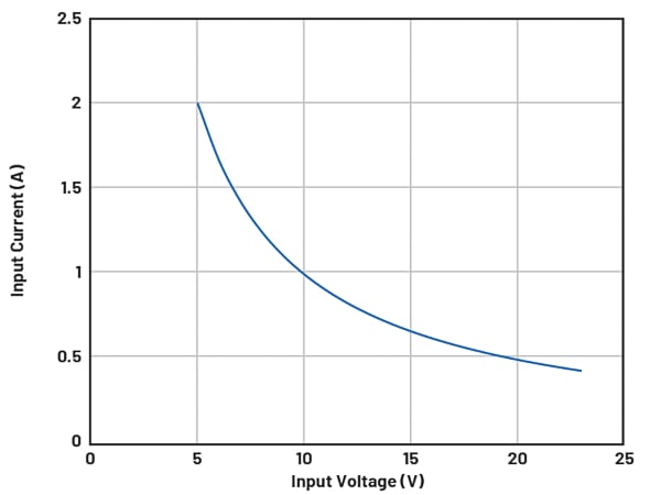
Figure 1. An input current as a function of the input voltage. Image used courtesy of Bodo’s Power Systems [PDF]
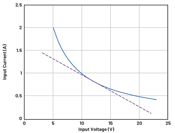
Figure 2. A tangent at 12 V was added. Image used courtesy of Bodo’s Power Systems [PDF]
Assume the regulator keeps the VOUT constant and the load current IOUT is considered as a constant and not a function of the VIN. Figure 1 shows the plot IIN as a function of VIN.
Figure 2, shows the tangent at the operating point 12 V. The slope of the tangent is equal to the small signal current change as a function of voltage in the operation point.
The slope of the tangent can be considered as the input resistance RIN or the input impedance RIN = ZIN (f = 0) of the converter. What happens with the input impedance for frequencies f > 0 is a later discussion in this article. For now, we assume its constant over frequency ZIN (f) = ZIN (f = 0). The most interesting observation is: This small signal input resistance is negative as the slope is negative. If the input voltage increases, the current decreases, and vice versa.
As a starting point, look at the circuit in Figure 3, where the SMPS, together with its input capacitance and inductance in the feed, forms a high Q LC circuit damped by a negative resistance. If the negative resistance dominates the circuit, it becomes an oscillator that will oscillate undamped close to the resonance frequency. In practice, nonlinearities in the large signal oscillation will affect the oscillating frequency and its waveform.
The inductor in this circuit may be the inductance of the input filter or cables. To make the circuit stable, positive resistance must dominate over negative resistance to make the circuit damped. This is problematic because you do not want the series resistance of the inductor to be high. This would increase the heat dissipation and reduce efficiency. The series resistance of the capacitor should not be too high because the voltage ripple will increase.
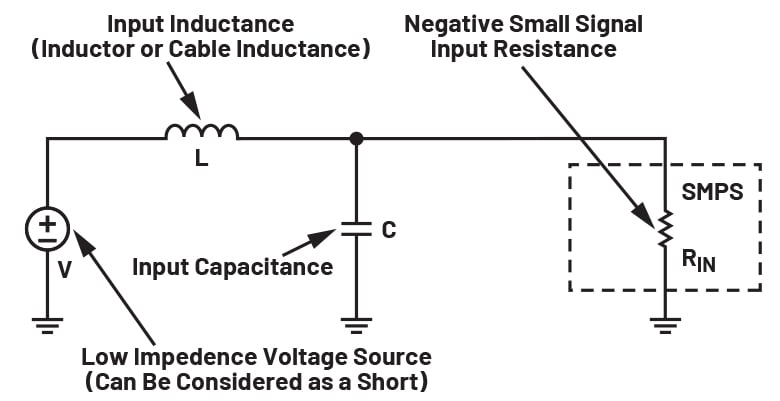
Figure 3. A small signal model of the SMPS and its input network. Image used courtesy of Bodo’s Power Systems [PDF]
Analyzing the Problem
When designing your power supply system, here are some questions that may arise:
- Do I have such a problem in my design?
- How do I analyze it?
- How do I solve it if there is a problem?
If we assume there is only one active element in the input circuitry acting as a negative resistance, we can analyze the impedance by looking directly into the input of the SMPS.
If the real part of the impedance is >0 over frequency, the circuit is stable, presuming the SMPS control loop itself is stable. The analysis can be done analytically or by simulation. Simulation can easily be used even if the input circuit has many elements while the analytic design is harder. We will start the simulation using LTspice.
Start with calculating the first-order approximation of the negative resistance by derivation of the formula:
\[I=\frac{P}{U}\rightarrow\frac{dI}{dU}=-\frac{P}{U^{2}}\rightarrow R=\frac{dU}{dI}\rightarrow R_{IN}-\frac{U_{IN^{2}}}{P_{IN}}\,\,\,\,\,\,(2)\]
If the input power of a converter is 30 W, at 12 V it will give you the resistance –122/30 Ω = –4.8 Ω. The input filter consists of an LC filter. Presuming the input is fed by a low ohmic power supply, the equivalent circuit may be simplified and boiled down to an example schematic in Figure 4 with an ideal 0 Ω supply.
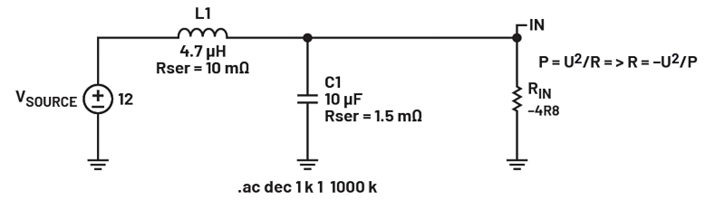
Figure 4. An SMPS and its input network example. Image used courtesy of Bodo’s Power Systems [PDF]
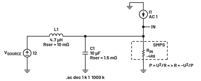
Figure 5. Current source stimuli (I1) added to the network. Image used courtesy of Bodo’s Power Systems [PDF]
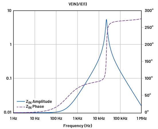
Figure 6. A simulation result of impedance at injection point. Image used courtesy of Bodo’s Power Systems [PDF]
If we add a current source to the simulation, we can calculate the small signal impedance at the input as V(IN)/I(I1). This is easily simulated in LTspice.
As we can see in the impedance graph, there is a resonance peak at about 23 kHz. The phase of the impedance goes into the range of 90°< phase <270° at around the resonance frequency of the LC circuit, which means the real part of the impedance is negative. We can also plot the impedance in Cartesian coordinates and see the real part directly. It is also notable that the real part gets quite large (–3 Ω) at the resonance due to the high Q.
Figure 7. The same impedance as shown in Figure 6 but in Cartesian coordinates. Image used courtesy of Bodo’s Power Systems [PDF]
A time domain simulation where a disturbance transient at time 1 ms is injected and results in the unstable behavior shown in Figure 8.
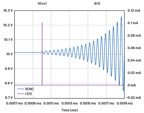
Figure 8. A simulation where a transient is injected at time 1 ms. Image used courtesy of Bodo’s Power Systems [PDF]
As mentioned earlier, we do not want to add serial resistance to the reactive parts in the design for obvious reasons. One thing we can do without negatively affecting the design (except for its size) is add a damping capacitor that has the same or larger capacitance magnitude with a series resistance that is appropriate to dominating the impedance at the frequency of interest. For a reasonable damping result, the size of that capacitor should be at least a small factor larger than the already present input capacitance. The series resistance should be significantly lower than the negative resistance of the SMPS, but equal to or larger than the reactance of the added capacitance at the problematic frequency. If a nonceramic bulk capacitor is added, its parasitic ESR may be good enough on its own assuming that there are margins for component variations.
How to Select a Damping Capacitor and Its Series Resistance
Either use trial and error in LTspice or, if the circuitry is simple, use the following analytic method to retrieve the values.
First, calculate the resonance frequency of the input capacitor and input inductance that can be considered to sit in parallel in between the input of the SMPS and AC ground if the supply on the other end of the inductor can be considered low ohmic in comparison with the input filter.
\[f=\frac{1}{2\times\pi\times\sqrt{L}\times C}t\,\,\,\,\,\,\,\,\,\,\,\,\,\,\,\,\,\,(3)\\
C=Total\,Filter\,Capacitance\\
L=Total\,Filter\,Inductance\]
At the resonance frequency, the absolute value of the reactance of the capacitor and inductance is equal.
\[|X_{L}|=|X_{C}|=\sqrt{\frac{L}{C}}\,\,\,\,\,(4)\]
The total parallel impedance at resonance will be defined by the following complex formula:
\[Z_{Parallel}=\frac{R_{L}\times R_{C}+JR_{L}X_{C}+JR_{C}\times X_{L}-X_{L}\times X_{C}}{R_{L}+R_{C}+JX_{L}+JX_{C}}\,\,\,\,\,(5)\]
\[X_{L}=Reactance\,of\,Inductor\\
X_{C}=Reactance\,of\,Capacitor\\
R_{L}=Series\,Resistance\,of\,the\,Inductor\\
R_{L}=Series\,Resistance\,of\,the\,Capacitor\]
As XL = –XC and RL and RC normally is much smaller than the reactance, the formula can be approximated and simplified.
\[Z_{Parallel}=\frac{-X_{L}\times X_{C}}{R_{L}+R_{C}}\,\,\,\,\,(6)\]
And, finally, enter the values for X = √L/C and X = –√L/C.
\[Z_{Parallel}=\frac{L}{C}\times\frac{1}{R_{L}+R_{C}}\,\,\,\,\,(7)\]
This is the equivalent parallel resistance of the input filter at resonance.
If this resistance is lower than the absolute value of the negative resistance of the SMPS, the positive resistance is dominating, and the input filter network will be stable.
If not, or there is little margin, damping must be added.
This can be done by the previously mentioned extra capacitor with series resistance selected for optimal damping. See R1 and C2 in Figure 9.
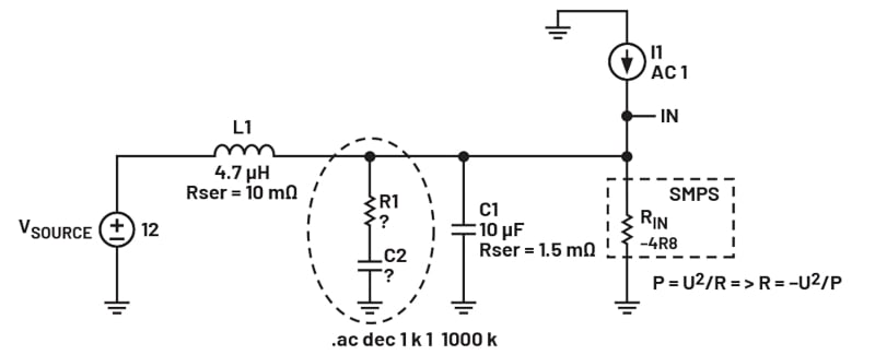
Figure 9. Damping networks R1 and C2 were added to the input. Image used courtesy of Bodo’s Power Systems [PDF]
The value of the extra capacitors must be of the same magnitude or larger than the filter capacitance. The reactance of the capacitor at the resonance frequency of the input filter must be significantly lower than the absolute value of the negative resistance of the SMPS, which is usually the case if the first condition is met.
The size of the extra capacitor is a compromise. One design objective could be to come close to critical damping of the input filter. This can be done by calculating the parallel resistance that would give critical damping, which happens when the parallel resistance is half the value of the reactance (Q = 1/2). That means the parallel resistance of the input filter in parallel with the negative SMPS resistance in parallel with the (negative) damping resistor RDAMP in question should be equal to half the reactance of the input filter C and L at resonance:
\[R_{DAMP}=\frac{1}{2}\times\frac{1}{\frac{1}{\sqrt{\frac{L}{C}}}-\frac{1}{\frac{L}{C}\times\frac{1}{R_{L}+R_{C}}}-\frac{1}{R_{IN}}}\,\,\,\,\,(8)\]
If the values of L/C × 1/(RL + RC) and |RIN| are much larger than √L/C, the formula can be simplified to:
\[R_{DAMP}=\frac{1}{2}\times\sqrt{\frac{L}{C}}\,\,\,\,\,(9)\]
In relation to the damping resistor, a reasonable size damping capacitor should be selected. XDAMP = 1/3 × RDAMP is a suggestion, which means CDAMP = 6 × C if the above assumption of L/C × 1/(RL + RC) and |RIN| is much larger than √L/C is still valid.
The input will not reach critical damping but is close. If more ringing can be tolerated and design margins are robust, a smaller C can be used. In our example
\[R_{DAMP}=\frac{1}{2}\times\sqrt{\frac{4.7\mu H}{10\mu F}}=0.69\Omega\,\,\,\,\,(10)\\
C=6\times10\mu F=60\mu F\]
Use 0.68 Ω and 68 μF as shown in Figure 10. The time domain response of a disturbance and AC impedance is shown in figures 11 and 12.
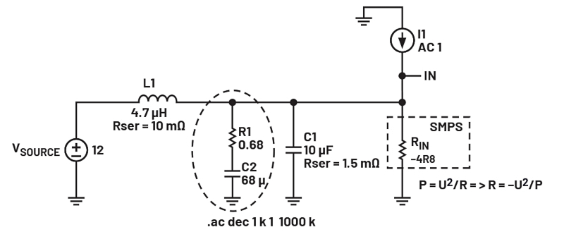
Figure 10. A damping network with suggested component values. Image used courtesy of Bodo’s Power Systems [PDF]
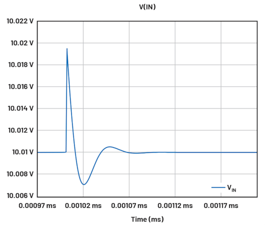
Figure 11. A time domain transient response. Image used courtesy of Bodo’s Power Systems [PDF]
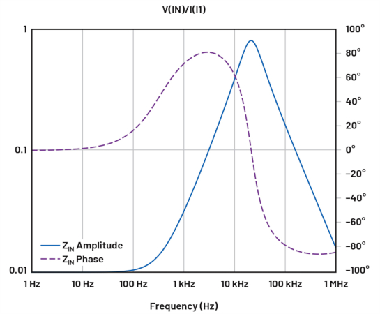
Figure 12. Impedance as a function of frequency. Image used courtesy of Bodo’s Power Systems [PDF]
Frequency Behavior of the Negative Resistance
You may assume that a power supply unit (PSU) will stop behaving as a negative resistance beyond the loop bandwidth of the control loop—but that is usually the wrong assumption. If the PSU is in current mode, the instant response on a positive input voltage change will be a duty cycle change maintaining the peak current value the regulator demands. This means the input current will momentarily decrease in case of a voltage increase and vice versa.
As a result, the negative resistance is maintained all the way up to the switching frequency. If the PSU is voltage mode-controlled, there is usually a feedforward function from the input voltage to the duty cycle that will make the converter respond immediately to the input voltage changes to keep the output voltage constant. This also results from the negative resistance being present all the way up to the switching frequency. The concussion is that reducing the control loop bandwidth does usually not solve the problem. Also, an unregulated bus converter can still look like negative resistance if downstream converters are regulated.
Takeaways of Oscillation in Power Supplies
Oscillation in power supplies due to poor input network matching may be mistaken for control loop instability. But if acknowledged as an input network and negative resistance-related oscillation, the behavior can be easily analyzed and optimized in LTspice. LTspice is a free high-performance SPICE simulator software, including a graphical schematic capture interface. Schematics can be probed to produce simulation results—easily explored through the LTspice built-in waveform viewer. The LTspice enhancements and models improve the simulation of analog circuits when compared to other SPICE solutions.
This article originally appeared in Bodo’s Power Systems [PDF] magazine.


Hello, Nice article with good insight. As a complementary piece of info for readers, may I suggest “Input Filter Design” for power supplies such as Chapter 10 of Fundamentals of Power Electronics, second edition, and similar resources? Thank you.