How to Operate a Transistor as a Switch
Transistor switches are vital to electronics. Learn about transistor switches, from their operating regions to more advanced characteristics and configurations.
Transistor switches are vital to electronics in the switching of low DC ON/OFF where the transistor is operated in its cut-off or saturated state. Some electronic devices, such as LEDs, require a few milliamps to power on and can be driven by the logic gate outputs. However, high-power electronic devices such as solenoids, lamps, and motors demand more electrical power than the logic gate supplies. Enter transistor switches.
Transistor Switch Operations and Operating Regions
The blue shaded area on the graph in Figure 1 represents the saturation region, while the pink shaded area represents the cut-off region.

Figure 1. Transistor Operating Region. Image used courtesy of Simon Munyua Mugo
The regions are defined as:
• Saturation region. This is the region where the transistor will be biased for the maximum amount of base current to be used to achieve maximum current at the collector and minimum voltage drop at the collector-emitter and which in turn makes the depletion layer as tiny as possible hence the flow of maximum current through our transistor. This makes the transistor switch ON. Figure 2 demonstrates the saturation region characteristics.

Figure 2. Saturation Region Characteristics. Image used courtesy of Simon Munyua Mugo
• Cut-off region. Here the input base current and the output collector current are zero and the collector voltage is at the maximum resulting in a large depletion layer with zero current flowing through the transistor. In such conditions, the transistor is switched off.
The cut-off region characteristics are shown below:

Figure 3. Cut-off Region Characteristics. Image used courtesy of Simon Munyua Mugo
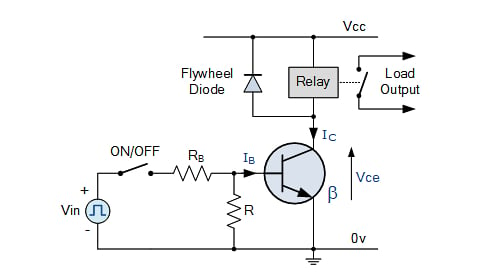
The transistor operation is similar to that of a single-pole single-throw solid state switch, where when zero signals are applied at its base, then it remains OFF and in such a situation, it acts as an open switch with zero collector current flowing. When we apply a positive signal to the base of the transistor, it is switched ON, and in this situation, it acts as a closed switch where maximum current flows through it.
Basic Transistor Switching Circuit

Figure 4. Basic NPN Transistor Switching Circuit. Image used courtesy of Simon Munyua Mugo
The circuit is similar to that of the Common Emitter circuit. The difference is that we need to turn the transistor fully ON (saturated) or fully OFF (cut-off) to be able to operate it as a switch.
An ideal transistor switch has infinite resistance between the Emitter and the Collector when it is turned fully-OFF leading to 0 current flow through it and 0 resistance between the Emitter and the Collector when fully-ON leading to the flow of current to the maximum.
Practically, we shall have a small number of leakage currents when the transistor operates at cut-off that is when fully-OFF. On the other hand, when operated at the saturation region, the device has low resistance leading to the flow of a small voltage we refer to as saturation voltage (VCE).
For the Base current to start flowing, the Base terminal must be more positive than the Emitter. For a silicon device, the Base must have a biasing input voltage of at least 0.7 volts. Varying the Base-Emitter voltage (VBE) alters the Base current which in turn varies the Collector current that flows through the given transistor.
If we attain the maximum flow of the Collector current, then the transistor is Saturated. The amount of input voltage and the current needed to put the transistor ON is determined by the Base resistor
Let us assume that
b=200, IC=6mA, and Ib=25uA
Find the Base resistor (Rb) value that is needed to fully power ON the transistor when the voltage at the input exceeds 3.0V
Solution
\(R_{b}=(V_{in}-V_{BE})/I_{B}\)
\(R_{b}=(3.0V-0.7)/25X10\)^\(-6\)
\(R_{b}=92k\Omega\)
The preferred lowest value that will guarantee a saturated transistor switch is 82kΩ.

Figure 5. Digital Logic Transistor Switch. Image used courtesy of Simon Munyua Mugo
In the circuit above Rb is required for limiting the output current from the digital logic gate.
PNP transistor Switch
A PNP transistor can be used in the same way as an NPN transistor. The difference is that in PNP, the load is always connected to the ground and the PNP will be used to switch power to the load. To turn the PNP transistor on, we must ground the base terminal as in Figure 6.

Figure 6. Switching Circuit of the PNP Transistor. Image used courtesy of Simon Munyua Mugo
The PNP transistor equation for calculation of the collector current, base resistance, and voltages are still the same used in the NPN calculations. The difference is the switching current. For PNP, the switching current is the sourcing current. For the NPN, it is the sinking current.
Darlington Transistor Switch
This involves the use of multiple switching transistors because there comes a time when the DC gain of a single bipolar transistor is too low to switch the load voltage or current. In the configuration, a small input bipolar junction transistor (BJT) transistor is involved in switching on and off a bigger current holding output BJT transistor.
For maximization of the signal gain, the two transistors are connected in a Darlington configuration which contains two NPN or PNP bipolar transistors interconnected such that the current gain of transistor 1 is multiplied by the current gain of transistor 2, ending up with a device that behaves like a single transistor with a higher current gain when a smaller base current is applied.
The total current gain value of this transistor is the product of the individual value of each transistor given by;
\[\beta_{TOTAL}=\beta_{1}\times\beta_{2}\]
Below are the possible Darlington Transistor Switch configurations.

Figure 7. NPN Darlington Configuration. Image used courtesy of Simon Munyua Mugo
In the NPN Darlington configuration, the collectors of the two transistors are connected while the base of the second transistor is connected to the emitter of the first transistor. From the configuration, we see that the emitter current of the first transistor becomes the base current of the second transistor that switches it on.
Key Takeaways for Using Transistor Switches
When using the transistors in switch applications, remember the following:
- When using BJTs, they must be either fully ON or OFF
- Transistor switches find use in the control of lamps, motors, and relays
- Fully ON transistors operate in the saturation region while fully OFF transistors operate in cut-off regions
- For the transistor to operate as a switch, a principle of the small base current controlling large collector load current is used.
- If you want to control large currents, use the Darlington transistor as a switch
Featured image used courtesy of Adobe Stock


