Facebook
 Google
 GitHub
 Linkedin
Avalanche Ruggedness of SiC MPS Diodes Under Repetitive Unclamped-Inductive-Switching Stress
This article highlights avalanche ruggedness of discrete 1.2 kV SiC MPS diodes.
Freewheeling diodes are connected antiparallel with a switch such as IGBTs or MOSFETs. They have to be rugged enough to overcome temporary overvoltage and overcurrent conditions. SiC merged pin Schottky (MPS) diodes are one of the superior contenders. The avalanche ruggedness of discrete 1.2 kV SiC MPS diodes from Infineon was investigated far beyond the specified maximum ratings. Furthermore, a repetitive avalanche was studied, including detailed failure analysis.
Introduction
Silicon carbide bipolar devices may suffer from forward voltage drift (VF) after bipolar current stress (bipolar degradation). The energy from electron-hole recombination causes Shockley type stacking faults (SSFs) which are triggered by basal plane dislocations and converted into triangular defects and bar-shaped stacking faults (BSSFs) [1][2]. The intention of this work is to investigate the possibility of recombination induced stacking faults (SFs) and other reliability issues under very high avalanche current.
Experiment Details
To perform UIS measurements, the test device was connected antiparallel to a 4.5 kV IGBT as shown in Figure 1. The applied DC link voltage has been varied in the range of 50 V to 900 V for different inductances. The diode current was measured with a coaxial high-power shunt. Optional resistance was connected in parallel to the inductance to reduce the LC oscillation. When the IGBT turns OFF, the stored energy in the inductance will cause a high voltage across the IGBT and the antiparallel connected test device. Since the rated voltage of the IGBT is higher compared to the device under test, the diode will go into avalanche mode with a high reverse current.

(a)

(b)
Figure 1: Test circuit (a) and typical schematics (b) of current and voltage waveforms in UIS measurements
Unclamped Inductive Switching
The avalanche behavior was measured with various inductances to find the avalanche limit of the test device as shown in figure 2 (a). The used inductance was between 12 μH to 3.1 mH with maximum avalanche energy (see Equation 1) deposited for the last pass pulse of 13.6 J/cm² to 11.8 J/cm² respectively. Due to the applied inductance, the total current (Itotal) and clamping time (tava) had changed (di/dt=VDC/L). The clamping time is shorter for lower inductance where the dissipated energy is stored only at the SiC bulk (for 3 μs). Whereas for higher inductance, due to longer tava, the dissipated energy could be transferred to the cathode side metallization layers.
Eava = ∫ Idiode(t). Vava(t)dt
The single event avalanche limit was measured for each inductance by increasing the DC link voltage until device destruction. After every UIS pulse, the forward and blocking behavior was tested to ensure the diode has not been destroyed during the pulse. As an example, a single event avalanche limit for 3.1 mH is shown in figure 2 (b). As the overvoltage occurs and the diode reaches Vava, the electric field is high and leads to avalanche multiplication [3], therefore, current flows in the reverse direction through the diode. After the avalanche regime, the diode returns to standard blocking mode. This can be seen in figure 2 (b) at VDC=908 V, the device goes into blocking after 11.5 μs. Increasing the DC link voltage to 920V, finally leads to the destruction of the device due to the exceedance of the maximum avalanche energy at 11 μs. The diode lost its blocking capability and a failure current flowing through the device and discharging the DC link capacitor.
Repetitive unclamped inductive switching An automated test bench was built for testing repetitive clamping [4]. The measurements were performed at ~30 to 40 percent below the single event failure limit and were made up to 100 k pulses with a 500 ms interval between each consecutive pulse. Every 20 k pulses, the test was interrupted to verify the forward voltage (VF), breakdown voltage (VBD) and Schottky barrier voltage (Vbi).

(a)

(b)
Figure 2: (a) Maximum avalanche energy (Eava) during the last pass pulse and maximum current (Itotal) as a function of inductance. (b) Last pass and destructive pulse of a single event UIS measurement with a load inductance of 3.1 mH

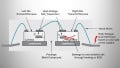
Figure 3: Repetitive avalanche stress under condition of L=3.1 mH; VDC=820 V; ton_(IGBT)=50 μs; tinterval=1 s; Tc=25°C
A repetitive UIS measurement was performed with inductances of 12 μH and 3.1 mH. The waveforms of the 3.1 mH condition are shown in figure 3. Since the avalanche time (tava) is longer, deeper layers of the device with more distance to the “active” drift zone could be heated up during the pulse. Therefore, a longer interval of one second between consecutive pulses has been applied in order to avoid heating effects. The temperature swing was calculated from the pre-calibrated temperature-dependent breakdown voltage [4]. In the case of short clamping time for 12μH, almost 100A were flowing through the diode during avalanche breakdown. The avalanche energy is Eava≈10 J/cm², which is an extreme condition for the diode. However, some of the diodes survived for 100 k pulses, see [4].
After 100 k repetitive UIS pulses, all test devices showed a forward voltage degradation, Schottky barrier lowering and an increase in the leakage current. Since the current peak and temperature swing is very high, another test device was subjected to avalanche stress (at L=3.1 mH) with lower dissipated energy Eava=2.7 J/cm² and a temperature swing of approximately ~65°C. Since the avalanche energy is lower, the test device showed stable behavior without any degradation even after 100 k
After 100 k repetitive UIS pulses, all test devices showed a forward voltage degradation, Schottky barrier lowering and an increase in the leakage current. Since the current peak and temperature swing is very high, another test device was subjected to avalanche stress (at L=3.1 mH) with lower dissipated energy Eava=2.7 J/cm² and a temperature swing of approximately ~65°C. Since the avalanche energy is lower, the test device showed stable behavior without any degradation even after 100 k pulses.

(a)

(b)

(c)
Figure 4: Failure patterns of the 1.2 kV SiC MPS after repetitive UIS tests. (a) and (b) after 100 k repetitive avalanche pulse without destruction. (c) failed test device during repetitive UIS measurement
Failure Analysis
In order to investigate the cause of degradation, the test devices were subjected to several failure analysis methods. To investigate possible stacking faults, some of the test devices which showed VF drift have been subjected to emission microscopy (EMMI) similar to [5]. For this purpose, the back-side lead frame was removed carefully. The tested devices were subjected to forward and reverse bias as shown in Figure 4 (a) and (b) respectively. A homogenous current distribution was observed across the chip surface, meaning no recombination induced stacking faults have occurred. A possible physical reason could be connected to the fact that at high electric field the drift velocity of the carriers becomes saturated. Hence, during avalanche multiplication with vsat=107 cm/s and base within the range of 10 μm, the carrier transit time wB/vsat is in the range of 0.1 ns which is too short for significant bipolar recombination. Consequently, no recombination can occur.
The p+ islands of the MPS diode are hardly visible from the EMMI picture due to a strong change in the Aluminium (Al) metallization. Therefore, the front-side covering mold compound was removed and inspected optically. Certain abnormal grains were observed on the front side metallization, see [4]. This metal surface modification could be caused due to the high-temperature swings during the repetitive UIS stress.
One example of a failed test device during repetitive UIS measurement is shown in figure 4 (c). The used TO-247 package consists of two diodes with a common cathode. The left side diode D1 was tested under the same conditions as shown in figure 3. However, in this case, the test device survived up to ~80 k pulses, then massive damage was observed in the middle of the chip. The chip was completely melted at the location of the bond wire due to very high avalanche energy far beyond the SOA of the device. The neighboring diode D2 was unaffected.
Conclusion
The measurements and extensive failure analysis show that the above-mentioned modifications and VF shift in the diode after repetitive UIS stress is due to change in the front side metallization by Al modification caused by the high-temperature swing. EMMI pictures show a homogenous current distribution and no stacking faults (SFs) are visible. Even at very high current peak (~100 A), no recombination induced SFs could be found since the transit time of carriers is too short for significant recombination.
In general, one can conclude that the 1.2 kV SiC MPS diodes from Infineon show high avalanche ruggedness even at extreme conditions, far beyond the specified maximum rating of the device.
References
[1] T. Kimoto et al., “Understanding and reduction of degradation phenomena in SiC power devices,” IEEE International Reliability Physics Symposium Proceedings, pp. 2A1.1-2A1.7, 2017.
[2] U.-L. and P. S. J.P.Bergman, H.Lendenmann, P.A.Nilsson, “Crystal Defects as Source of Anomalous Forward Voltage Increase of 4H-SiC Diodes,” Materials Science Forum, vol. 353–356, pp. 299–302, 2011.
[3] T. Hatakeyama, “Measurements of impact ionization coefficients of electrons and holes in 4H-SiC and their application to device simulation,” Physica Status Solidi (A) Applications and Materials Science, vol. 206, no. 10. pp. 2284–2294, 2009.
[4] S. Palanisamy, M. K. Ahmmed, J. Kowalsky, J. Lutz, and T. Basler, “Investigation of the avalanche ruggedness of SiC MPS diodes under repetitive unclamped-inductive-switching stress,” Microelectronics Reliability, vol. 100–101, no. July, p. 113435, 2019.
[5] R. Rupp et al., “Avalanche behaviour and its temperature dependence of commercial SiC MPS diodes: Influence of design and voltage class,” Proceedings of the International Symposium on Power Semiconductor Devices and ICs, pp. 67–70, 2014.
About the Authors
Shanmuganathan Palanisamy received his Diploma in Electrical and Electronics Engineering at the Department of Technical Education Chennai India, Bachelor of Engineering in the Field of Electrical and Electronics Engineering at Anna University, and Master of Science in the Field of Micro and Nano Systems at the Technical University of Chemnitz. He is an experienced engineer with a demonstrated history of working in the higher education industry. Skilled in Power Semiconductors, Silicon Carbide, and Power devices.
Thomas Basler is a researcher who worked in Industrial Power Control at Infineon Technologies.