Facebook
 Google
 GitHub
 Linkedin
Using Coupled Inductors To Increase Power Density in DC-DC Apps
This article examines an enhancement to traditional buck topology in 48 V distribution in data centers and communication applications.
This article is published by EEPower as part of an exclusive digital content partnership with Bodo’s Power Systems.
Forty-eight-volt distribution is popular in data center and communication applications, with many solutions for the step down from 48 V to the intermediate rail. The simplest approach is a buck topology, which can provide high performance but often falls short in power density. Upgrading the multiphase buck with coupled inductors enables a dramatic power density improvement that matches the state-of-the-art alternatives while keeping the massive performance advantage.
The multiphase coupled inductors have inverse coupling between windings, enabling current ripple cancellation in each phase current. This benefit can be traded either for efficiency or, for example, size reduction and power density improvement.
The 48 V distribution rail is typically stepped down to some intermediate voltage, often 12 V or lower. Then, the different local point-of-load regulators deliver different voltages directly to different loads. One of the first choices to consider for the step-down voltage regulator 48 V to 12 V is a multiphase buck converter (Figure 1). This solution has regulated VO and fast transient, which is simple and inexpensive. For a power range of a few hundred watts to >1 kW, four parallel phases can be considered. However, as high efficiency is often a priority, switching frequency is often relatively low for the 48 V converters to keep the switching losses down, compared to the lower voltage applications with 12 V or even 5 V input. This hurts magnetics twice in terms of volts × seconds, as the already noticeable voltage is also applied for a relatively longer time. As a result, magnetics for 48 V are typically bulky, with multiturn windings to withstand the significantly increased volt × seconds compared to lower voltage applications. High efficiency can still be achieved in a 48 V buck converter, but typically with a significant overall size, where inductors occupy most of the volume.
The basic 48 V to 12 V ~1 kW buck converter has four phases with discrete inductors 6.8 μH and switches at 200 kHz. These four inductors are the biggest and tallest components, representing most of the solution volume.
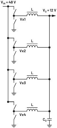
Figure 1. Four-phase buck converter with discrete inductors. Image used courtesy of Bodo’s Power Systems [PDF]
Current Ripple
The current ripple in each phase of the conventional buck can be found in Equation 1, where the duty cycle is D = VO/VIN, VO is the output voltage, VIN is the input voltage, L is the inductance value, and Fs is the switching frequency.
\[dIL_{DL}=\frac{V_{IN}-V_{O}}{L}\times\frac{D}{F_{S}}\,\,\,(1)\]
Replacing the discrete inductors (DL) with the coupled inductor1–7 that has a leakage inductance Lk and the mutual inductance Lm, the current ripple in CL (coupled inductor) can be shown as Equation 2.6 The FOM is expressed as Equation 3, where Nph is the number of coupled phases, ρ is a coupling coefficient (Equation 4), and j is a running index, which just defines an applicable interval of the duty cycle (Equation 5).
\[dIL_{DL}=\frac{V_{IN}-V_{O}}{L}\times\frac{D}{F_{S}}\times\frac{1}{FOM(D,N_{ph,\rho,k})}\,\,\,(2)\]
\[FOM=\frac{\Big(1+\frac{\rho}{\rho+1}\times\frac{1}{N_{ph}-1}\Big)}{1\Biggr[(N_{ph}-2\times j-2)+\frac{j\times(j+1)}{N_{ph}\times D}-\frac{N_{ph}\times D\times(N_{ph}-2\times j-1)+j\times(j+1)}{N_{ph}\times(1-D)}\Biggr]\times\frac{\frac{\rho}{\rho+1}}{N_{ph}-1}}\,\,\,(3)\]
\[\rho=\frac{L_{m}}{L_{k}}\,\,\,(4)\]
\[j=floor(D\times Nph)\,\,\,(5)\]
Coupled Inductor Considerations
The first step for the improvement would be to plot a FOM for the Nph = 4 for several practically reasonable values of the coupling coefficient Lm/Lk (Figure 2). The red curve Lm/Lk = 0 represents FOM = 1 baseline for the discrete inductor. It was shown that the notch CL (NCL) structures with very low leakage can generally achieve very high Lm/Lk and, therefore, high values of FOM.8,9 However, while the duty cycle of interest is ideally right in the first notch D = 12 V/48 V=0.25, it is necessary to consider some range for the VIN and VO. Sometimes, the nominal VIN can be 48 V or 54 V plus some tolerance, VO can be adjusted away from 12 V, etc. For the current ripple to remain contained if the duty cycle changes around D = 0.25 in some range, a typical CL design with significant leakage is chosen instead of NCL, still with a significant FOM value. Assuming Lm/Lk > 4, a benefit of ~6× could be considered from FOM in Figure 2 to decrease the inductance value in CL, compared to the DL baseline. Decreasing the energy storage should directly affect the required volume of the magnetics. Reducing DL = 6.8 μH value to CL = 1.1 μH should, therefore, be beneficial for the size reduction.
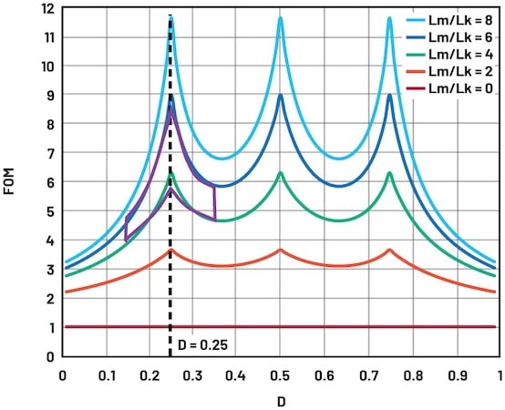
Figure 2. FOM for a 4-phase CL for some different Lm/Lk values as a function of the duty cycle D. The region of interest is highlighted. Image used courtesy of Bodo’s Power Systems [PDF]
The corresponding current ripple is plotted in Figure 3, comparing baseline design DL = 6.8 μH with proposed 4-phase CL = 4 × 1.1 μH (Lm = 4.9 μH) at VIN = 48 V and Fs = 200 kHz conditions. In the region of interest, the current ripple of CL is similar to or smaller than that of DL. This implies that the rms of all circuit waveforms are similar, and so are the conduction losses. The same ripple at the same Fs also implies the same switching losses, gate drive losses, etc., which means that the efficiency between the two solutions should be very similar (assuming a similar contribution from DL and CL inductor losses, as the only difference).
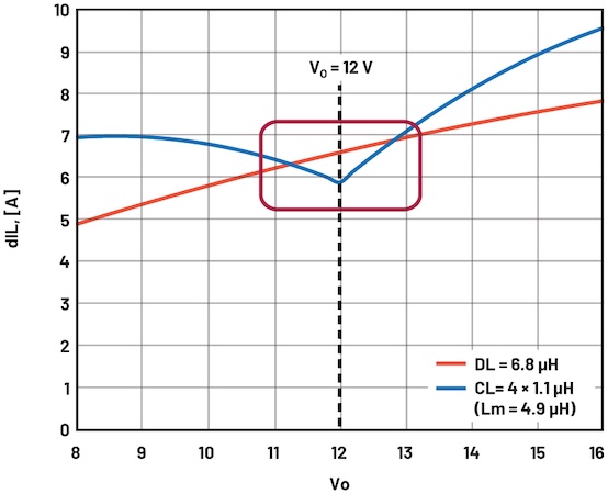
Figure 3. Current ripple for DL = 6.8 μH and CL = 4 × 1.1 μH for VIN = 48 V and Fs = 200 kHz as a function of VO. The region of interest is highlighted. Image used courtesy of Bodo’s Power Systems [PDF]
Designed CL = 4 × 1.1 μH is shown in Figure 4, replacing four DL = 6.8 μH inductors.5 Each DL is 28 mm × 28 mm × 16 mm, assuming they are spaced 0.5 mm apart: 4-phase CL with 56.5 mm × 18 mm × 12.6 mm dimensions achieves 4× volume reduction for magnetics.
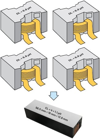
Figure 4. Four DL = 6.8 μH inductors (top) are replaced with CL = 4 × 1.1 μH (bottom), achieving 4× volume reduction. Image used courtesy of Bodo’s Power Systems [PDF]
A complete 1.2 kW 48 V to 12 V regulated solution is shown in Figure 5. The CL dimensions and footprint are purposefully designed to fit two CL parts inside an industry-standard quarter-brick size. Placing all ~1 mm components (FETs, controller ICs, ceramic capacitors, etc.) on the bottom side of the PCB enables a 1/8-brick size for the 1.2 kW solution.
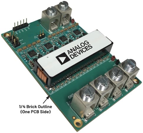
Figure 5. 48 V to 12 V regulated first stage. Components are placed on the top PCB side inside the 1/4-brick outline. Moving all ~1 mm components to the bottom: 1/8-brick. Image used courtesy of Bodo’s Power Systems [PDF]
Performance Gain
When the DL = 6.8 μH inductors were changed to CL = 4 × 1.1 μH—the current slew rate limit in the inductor also improved by 6×, which is always helpful for transient improvement. On top of this, the inductor saturation rating improved by ~2× at 100°C, even though the total magnetics volume decreased by 4×.
The transient performance of the proposed VIN = 48 V solution with the VO = 12 V output is illustrated in Figure 6. As expected, feedback regulates the output voltage to a preset value for the changing load current, compensating for any changes in the input voltage.
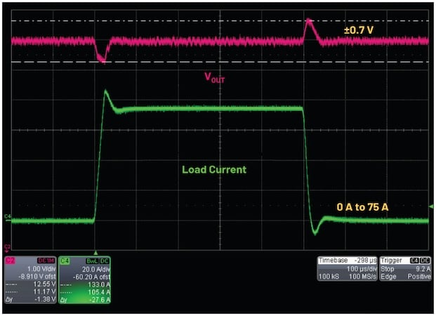
Figure 6. Transient at the VO = 12 V output (CL = 4× 1.1 μH) for the 75 A load steps. Image used courtesy of Bodo’s Power Systems [PDF]
Perhaps the most important performance parameter, achieved efficiency, is shown in Figure 7. It is compared to the state-of-the-art industry solution: 48 V to 12 V (fixed 4:1 step down) LLC with matrix transformer and GaN FETs on both primary and secondary sides. Compare the achieved full load efficiency of 97.6% and the benchmark of 96.3%. This implies that 16.6 W less losses are dissipated at full power, reaching 1.6 times improvement in the proposed solution. Such loss reduction is typically very hard to achieve when the efficiency is already high.
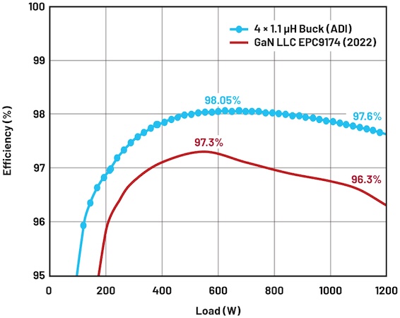
Figure 7. Efficiency comparison of the state-of-the-art 48 V to 12 V solutions in 1/8-brick form factor. Image used courtesy of Bodo’s Power Systems [PDF]
A trade-off between size and efficiency is certainly possible. Figure 8 compares the efficiency of the CL = 4 × 1.1 μH (4× reduction in magnetics size compared to DL) to a larger CL = 4 × 3 μH with only 2× reduction in inductor volume. The physically larger CL = 4 × 3 μH has a higher Lk = 3 μH value for leakage and a larger mutual inductance Lm = 10 μH. This allows a comfortable Fs reduction to 110 kHz, pushing the efficiency significantly higher in a whole load range.
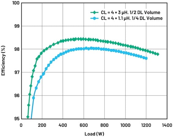
Figure 8. Efficiency vs. size trade-off for the proposed 48 V to 12 V solution with coupled inductors. Image used courtesy of Bodo’s Power Systems [PDF]
Takeaways
Utilizing the coupled inductor benefits, the 48 V to 12 V solution reduces the total magnetics size by 4× from the base discrete inductors, achieving 1.2 kW in the industry standard 1/8 brick form factor. This 4× magnetics size reduction is achieved while preserving the excellent efficiency performance, increasing inductor current slew rate in transient by 6×, and increasing inductor Isat rating by 2×.
Compared to the industry state-of-the-art 48 V to 12 V solution in the same form factor, ~1.6× loss reduction is achieved at full power. Efficiency is shown to improve further if a smaller reduction in magnetic size is acceptable.
At the same time, the proposed solution is fully regulated and placed directly on the customer's motherboard. It also utilizes standard silicon FETs to optimize the cost further. This is compared to unregulated 4:1 LLC, with all GaNFETs manufactured as a separate module with a specialized PCB with many layers, a sensitive layout, and an embedded matrix transformer.
The overall performance gain illustrates the advantages of ADI’s patented IP on coupled inductors in DC-to-DC applications.
This article originally appeared in Bodo’s Power Systems [PDF] magazine and is co-authored by Alexandr Ikriannikov, Fellow, and Laszlo Lipcsei, Director of Product Applications, with Analog Devices.