Facebook
 Google
 GitHub
 Linkedin
What Current-Mode Gate Drivers Mean for Wide Bandgap Devices in Data Center Power
AI's demand for power density drives the need for smaller, integrated gate drivers. High-voltage designs using wide bandgap transistors often face footprint challenges.
This article is published by EEPower as part of an exclusive digital content partnership with Bodo’s Power Systems.
The rapidly increasing power density demanded by artificial intelligence workloads is pushing the industry toward smaller and more integrated gate driving solutions. However, many AC-DC and DC-DC designs require four or more high-voltage wide bandgap transistors in each stage, which makes the isolated gate driver selection a significant footprint concern.
Data center power supplies have ever-increasing efficiency requirements, and achieving the highest efficiency requires driving the transistors aggressively, which increases the current flowing into the parasitic capacitances of the devices. If this displacement current forces the gate-source voltage above its threshold, parasitic turn-on can occur. In the best case, this leads to a loss of efficiency. In the worst case, it can result in permanent and sometimes catastrophic failure.

Image used courtesy of Freepik
When a dv/dt is applied to the FET’s drain, the parasitic Miller capacitance, CGD, and the gate-to-source capacitor, CGS, are in series. The combination forms a capacitive divider with the gate node being the output. Assuming that the gate node is left floating, the approximate gate voltage rise can be approximated with \(dV_{GS}\approx\frac{C_{GD}}{C_{GS}}dV_{DS}\). The capacitance ratio, \(\frac{C_{GD}}{C_{GS}}\), and the VDS slew rate directly affect the possibility of parasitic turn-on. If VGS rises above VGS(th) then parasitic turn-on can occur. This is especially pertinent for high-electron-mobility transistors (HEMTs) such as SiC and GaN, which have low VGS(th).
Eliminating Engineering Tradeoffs
Traditional Voltage Mode Drivers (TVMDs), without a Miller clamp, will sink the Miller current through their pull-down network, which typically consists of an internal NMOS transistor and an external user-selected gate resistor. To achieve the best clamping of VGS from this Miller current, RGOFF will need to be minimized. However, this means that an engineering tradeoff needs to be made because with a low RGOFF, the turn-off dv/dt will be very large, potentially causing excessive VDS overshoot.
To prevent the possibility of parasitic turn-on, designers can employ a range of remedies, such as slowing the turn-on dv/dt, utilizing a negative gate drive voltage, or implementing a Miller clamp. Slowing down the turn-on dv/dt means that the switching losses will be higher, leaving untapped efficiency on the table. Utilizing a negative gate drive voltage incurs additional BOM and design complexity while also increasing the external power device’s body diode losses. Integrated Miller clamps increase the driver pin count and are usually only available on single-channel gate drivers. External Miller clamps allow the use of larger discrete devices for stronger clamping, but they take up more board area, add to driver pin count, increase BOM, and decrease reliability.
To address these issues, a new current-based gate drive technology called SelVCD™, which stands for Selectable Variable Current Drive, has been incorporated into Skyworks’ latest series of isolated gate drivers. Instead of using the usual PMOS pull-up and NMOS pull-down networks found in TVMDs, this approach uses controlled current sources to charge and discharge the gate. This removes the need for external gate resistors, allowing the driver to apply its full pull-down strength during transient conditions, improving immunity to parasitic turn-on.
The source and sink currents are independently adjustable via two pins, SPD+ and SPD-, allowing real-time tuning from the logic input side. SPD+ controls the sourcing output current, and SPD- controls the sinking output current. These settings can be dynamically updated across eight levels to optimize performance under changing conditions such as bus voltage, load current, and temperature. Control signals are transmitted across the capacitive isolation barrier and decoded on the output side.
The SelVCD architecture includes a built-in Miller clamp that engages whenever the output voltage falls to approximately 2 V above the gate driver’s ground. At this point, the driver overrides the user-selected SPD-setting and applies the maximum pull-down current (SPD- 7, up to 4 A for the UVLO 15 variant devices), maintaining this state until the next rising logic input transition.
Putting SelVCD to the Test
To show the benefit of the SelVCD-enabled Miller clamp, a half-bridge test setup was constructed utilizing two Wolfspeed 1200 V 16 mΩ SiCFETs (C3M0016120K) with TVMD and SelVCD gate drivers being compared, as shown in Figure 1. The high side gate driver is pulsed to apply a dv/dt to the low side FET’s drain. The low-side FET is attempted to be kept off utilizing the gate driver.
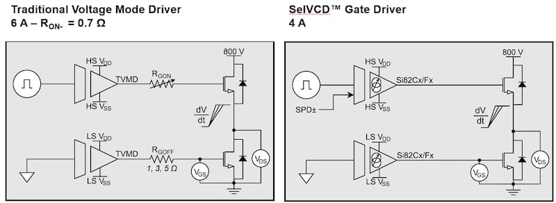
Figure 1. No current, dv/dt Miller clamp testing. Image used courtesy of Bodo’s Power Systems [PDF]
The FET’s datasheet requests a turn-on voltage of +15 V and a turn-off voltage between -3 to -4 V. However, to show the benefit of SelVCD, a 0 V turn-off voltage was used.
A 6 Amp TVMD with an internal pull-down RDSON of 0.7 Ω was utilized. In the TVMD case, the turn-on speed is varied by changing the RGON, and in the SelVCD gate driver case, the SPD+ setting is varied from SPD+ 0 to SPD+ 7. For the low-side gate driver, the RGOFF is varied between typical gate resistors of 1, 3, and 5 Ω, while the SelVCD gate driver is directly tied to the gate of the SiCFET.
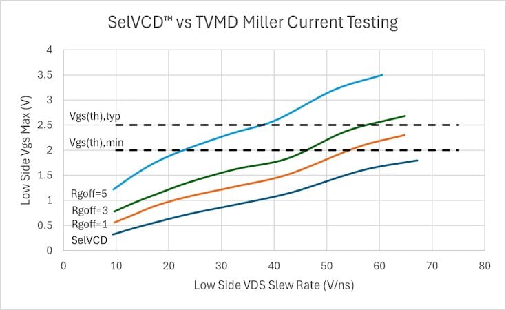
Figure 2. Parasitic Turn-On Testing Results. Image used courtesy of Bodo’s Power Systems [PDF]
As shown in Figure 2, the traditional voltage-mode gate driver, in every case, will eventually have the possibility of parasitic turn-on. SelVCD™ allows the gate to remain under the VGS(th),min condition even at the most extreme slew rates.
A customer was shown the previously discussed results and requested validation of their power factor correction (PFC) board, which uses two 750 V SiC FETs. These devices require +18 VGS,ON and 0 VGS,OFF. The existing design employed a 4.7 Ω turn-on resistor and a 2.2 Ω turn-off resistor, and the customer requested a comparison. Miller clamp testing was conducted at room temperature across four load conditions, as summarized in Table 1.
Table 1. Double Pulse Test Miller Current Test Conditions.
| Condition | Bus Voltage (V) | Load Current (A) |
| 1 | 227 | 25 |
| 2 | 455 | 25 |
| 3 | 227 | 45 |
| 4 | 455 | 45 |
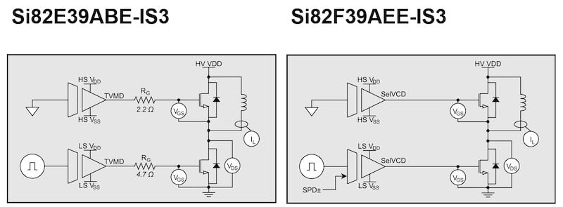
Figure 3. Miller clamp testing during double pulse test. Image used courtesy of Bodo’s Power Systems [PDF]
As shown in Figure 3, the low side is pulsed as in a double pulse test, and the high side VGS is viewed using an optically isolated probe. Specifically, the high-side VGS is viewed during the low side’s turn-on transition, which causes the high-side FET to have current injected into the parasitic Miller capacitor when VDS,HS goes from 0 V to 800 V. The SPD+ setting (SPD+ 4) of the low-side SelVCD gate driver was selected such that the falling VDS,LS slew rate was tightly matched to the 4.7 Ω TVMD driver. Both slew rates were within 2 V/ns of each other over all conditions tested.
As seen in Figure 4, the TVMD with the customer’s current gate resistor selections would need a negative gate drive rail to mitigate parasitic turn-on. However, this specific FET has an absolute maximum negative VGS of -4 V. Due to other transients affecting VGS, the only solution that would work for this FET with the TVMD is to slow down the turn-on transition, increasing the switching losses. However, the SelVCD driver stays well below the minimum VGS(th), mitigating these issues with no extra BOM required.
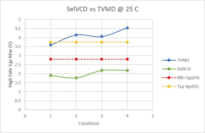
Figure 4. Double pulse test Miller clamp results. Image used courtesy of Bodo’s Power Systems [PDF]
Conclusion
SelVCD minimizes the risk of parasitic turn-on while allowing removal of the negative gate-drive bias. This allows users to lower their BOM, free up valuable board space, and improve system efficiency. To achieve comparable performance, TVMDs must rely on Miller clamps, reduced switching speeds, or negative gate drive voltages, all of which introduce design tradeoffs.
This article originally appeared in Bodo’s Power Systems [PDF] magazine.