Facebook
 Google
 GitHub
 Linkedin
Snubber Network Choices, Design and Evaluation
Power conversion circuits use snubber networks extensively to control voltage overshoots, improve efficiency and minimize EMI. This article discusses some circuit options and the design basics. Measurement of snubber performance is also discussed, with examples of pitfalls and best techniques for accurate results.
Power electronics has a variety of antiquated terms, some dating back centuries and perhaps ‘snubber’ is one, derived from Middle English which was spoken until the 15th century. The meaning of the word was originally to ‘scold’ or ‘curse’ but is now taken to indicate ‘cutting short’ or ‘damping’ in the electronics context. Specifically, a snubber is usually a network of components used to control and limit voltage or current excursions and is seen protecting the coils of relays and across semiconductor switches and rectifier diodes. Snubbers can also limit voltage and current edge rates, reduce EMI, limit power dissipation stress in semiconductors and reduce total switching losses, all dependent on the power conversion topology chosen and complexity of snubber. A typical RCD snubber network is shown in Figure 1, here used in an off-line flyback converter.
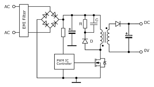
Figure 1. A common RCD snubber network in an off-line flyback converter. Image used courtesy of Bodo’s Power Systems
Snubber effects
The common use for a snubber is to limit voltage transients due to circuit parasitic effects. Switching power converters operate with pulsed current (i) by their nature and when this passes through transformer leakage or connection inductance (L), a voltage (V) is generated from the familiar relationship V = -L.di/dt. This impulse voltage causes ringing between the inductance and circuit capacitances, typically at a frequency of tens of MHz, with a peak value that can add hundreds of volts to the normal expected circuit value. The ring is typically non-sinusoidal due to the non-linear characteristic of switch capacitances with voltage. Modern wide band-gap semiconductor switches can operate with a di/dt of 2kA/µs or more, producing 2V for every nanohenry of inductance, and a transformer can easily have microhenries of leakage. Even a TO-247 transistor package has around 10-20nH inductance internally. In practice, such high current edge-rates are often deliberately slowed by other means such as gate resistors or inserted drain-gate capacitance, to make circuits practical and to prevent excessive EMI, but at the expense of some conversion efficiency. A snubber damps, and in this case also clamps the ringing voltage, which is reduced in amplitude and duration. Figure 2 shows the ringing that might occur in the circuit of Figure 1, without and with a snubber.
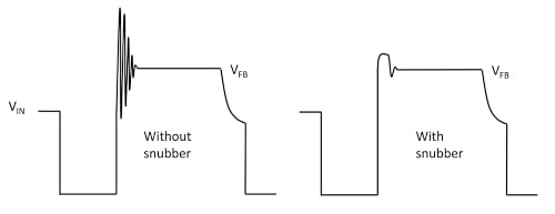
Figure 2. Typical switching waveforms of Figure 1 without and with a snubber. Image used courtesy of Bodo’s Power Systems
The damping and voltage clamping effect of a snubber is achieved by diverting energy into the capacitor in the network and slowing the voltage edge-rate. This can also serve to reduce switch dynamic losses by separating the overlap of current and voltage in a ‘hard’ switched converter, reducing the transient, high dissipation that occurs.
Snubber choices
Before a snubber is chosen and dimensioned, it is normally beneficial to investigate why the level of overshoot and ringing is present. Good transformer design can minimize leakage inductance and interleaving of windings can reduce it substantially; simply ‘sandwiching’ a transformer secondary between two primary windings can reduce leakage by a factor of around four compared with a single primary. Circuit track and connection inductances can also be minimized by good, compact layout. As a general rule, if the frequency of ringing is less than 100x the converter switching frequency, the cause should be examined first, as an effective snubber is likely to dissipate excessive power. It is also the case that there is no ‘correct’ snubber type and values – practical designs are always a compromise between acceptable component stress, EMI, snubber dissipation, cost and complexity.
A simple RC snubber (Figure 3A), is often used directly across a switch or diode to damp oscillations which occur at a frequency set by the device capacitance and circuit inductance. In the case of the MOSFET in the figure, this is output capacitance Coss and LLK, the transformer leakage inductance. LLK can be measured relatively easily, by shorting all transformer windings except the primary and measuring the resulting primary inductance. This is likely to be more dominant than connection inductance in practical circuits. Frequency of the ringing fR can be observed and from that, the characteristic impedance (Z) of the resonant circuit can be established:
$$Z = 2\cdot\pi\cdot {f_{R}}\cdot L_{LK}$$
Equation 1.
This is the starting point for the resistor value in the snubber network which forms the damping action. The capacitor blocks current from the DC rail and is a value that allows the resistor to be effective, while minimizing dissipation at the switching frequency. A value C, that gives the same impedance as the resistor at the ring frequency is a starting point.
$$C = 1/(2\cdot \pi\cdot f_{R}\cdot Z)$$
Equation 2.
The power dissipated P in the resistor, is determined from the energy expended charging and discharging the capacitor each switching cycle from zero to V, the sum of input and flyback voltage VFB. Dissipation is given by:
$$P = C\cdot V^{2}\cdot f_{s}$$
Equation 3.
Note that the dissipation does not depend on resistor value. If P is too high, a smaller capacitor will be necessary with a higher consequent ring voltage. Some simple flyback circuits operate in variable frequency ‘boundary’ conduction mode, where the PWM frequency can go very high at light load. This can cause excessive snubber dissipation and make light load efficiency very poor.
A ’rule of thumb’ sometimes used to get starting component values, is to add a capacitor on its own that is observed to half the ring frequency, then a resistor is added to show acceptable damping of the ring waveform.
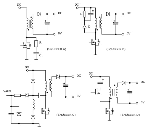
Figure 3. A selection of snubber circuits – simple RC (A), RCD (B), lossless passive (C), active clamp (D). Image used courtesy of Bodo’s Power Systems
The RCD snubber network (Figure 3B), provides a more secure clamping action of drain voltage and is preferred when the peak voltage expected at high line is close to the maximum for the switch. This is common in off-line converters where 650V rated devices are used for their availability and economy. In this circuit, operating in discontinuous conduction mode (DCM), when the MOSFET turns off and the drain voltage flies higher than the DC input rail, the diode conducts and charges the capacitor to the flyback voltage VFB. If the capacitor is large enough, it will remain at this nominal voltage over each switching cycle, absorbing ripple current from the ringing waveform. As a starting point for the design, note that the voltage VLK across LLK after the switch turns off and the diode conducts is the capacitor voltage, less the flyback voltage on the transformer primary:
$$V_{LV} = V_{CAP}-V_{FB}$$
The current through LLK is a downward ramp, with slope:
$$i/t = -V_{LV}/L_{LK} = -(V_{CAP}-V_{FB})/L_{LK}$$
Current (i) starts at the peak value of the transformer magnetizing current iPK and the linear ramp has a duration tSN , so substituting and rearranging:
$$i/t = t_{SN} = i_{PK}\cdot L_{LK}/(V_{CAP}-V_{FB})$$
The average current during the linear ramp is iPK/2 and over a switching cycle it is (iPK/2) multiplied by (tSN/tC), where tC =1/fS. We can now say that the power to be dissipated PSN in the snubber in a switching cycle is:
$$P_{SN} = (i_{PK}/2)\cdot(t_{SN}/t_{C})\cdot V_{CAP} = (i_{PK}/2)\cdot (t_{SN}\cdot f_{S})\cdot V_{CAP}$$
Substituting tSN:
$$P_{SN} = L_{LK} \cdot i_{PK}{^{2}}\cdot V_{CAP}\cdot f_{S}/(2\cdot (V_{CAP}-V_{FB}))$$
VCAP is chosen so that VCAP + VFB + VIN(max) does not exceed the switch breakdown rating with a good margin and all the other parameters are set by the circuit, while LLK can be measured. The resistor value R, to give this dissipation is given by:
$$R=V_{CAP}{^{2}}/P_{SN}$$
The capacitor value is not critical and is chosen for a ripple voltage, producing a maximum permissible ripple current through the component’s ESR and consequent heating. The component will typically be a polypropylene type for low loss. The ripple ΔVCAP is given by:
$$\Delta V_{CAP} = V_{CAP}/C.R.f_{s}$$
The diode should be a fast recovery type to avoid significant discharge of the capacitor as the diode becomes reverse biased. Forward recovery should also be low, as it adds a few volts to the clamped value.
For circuits operating in continuous conduction mode (CCM), and for forward or ‘buck’ derived circuits, the selection of components for an RCD clamp is similar and design equations can be found in the literature.
There are many more versions of snubbers that can be applied to switches including the circuit shown in Figure 3C. This is a ‘lossless’ snubber that ‘recycles’ the clamped energy. It can also be arranged for the energy to contribute to the power supply low voltage auxiliary rail for further power savings.
Other snubbers take the form of ‘active clamps’ which typically use MOSFETs to clamp the over-voltage (Figure 3D). The MOSFET usually requires a ‘high-side’ drive, offset from ground, but control ICs are available with this built-in. The circuit is similar to the active clamp used in forward converters to provide efficient transformer reset.
Example and evaluation of an RC snubber performance
The designs described assume that the leakage inductance can be measured, ideally at the switching frequency. This can be done in many circuits with an impedance analyzer or precision LCR bridge. However, the leakage inductance can sometimes be a low figure, which can be difficult to measure, especially in non-isolated power converters, where track and connection inductances dominate. Or sometimes, there is no LCR bridge or impedance analyzer available in the lab. In this case, inductance can be inferred by observing the ring waveform and adding an extra known capacitance C2 to the existing switching node capacitance C1 and observing the change in ring frequency.
As an example, a rectifier diode in a converter operating at about 38.5KHz without snubbing was observed to ring under reverse bias at a frequency f1 of 25.584MHz as shown in Figure 4. An additional capacitor of actual measured value 178pF was added and the frequency of the ring shifted to f2 or 21.9Mhz (Figure 5). At the two resonant conditions, the leakage inductance is constant so it can be stated:
$$L_{LK}=1/(4.\pi{^{2}}.f1{^{2}}.C1) = 1/(4.\pi{^{2}}.f2{^2}.(C1+C2))$$
Solving for C1 gives 488pF
Solving for LLK gives 108nH
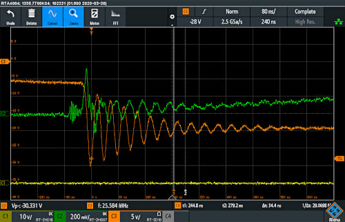
Figure 4. A measured switching diode waveform with no snubber. Image used courtesy of Bodo’s Power Systems
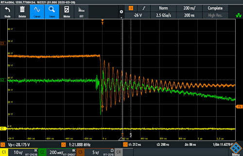
Figure 5. As Figure 4 but with known 178pF capacitor added. Image used courtesy of Bodo’s Power Systems
From Equation 1, if we assume the ring frequency will remain around 23MHz, the snubber resistor Rsnub starting value for critical damping would be around 16 ohms. However, a value of 35 ohms is chosen for slight under damping while still limiting the peak voltage to a safe value of around 27V. From Equation 2, with Z = 35 ohms, Csnub = 197pF and a standard value of 180 pF is chosen. From Equation 3, dissipation in Rsnub is just 5mW. At high voltages, the power can be significantly higher although some proportion is dissipated in the switch as it transitions through its linear region. The result is the waveform shown in Figure 6 showing voltage limited to a safe value and faster damping of the ring.
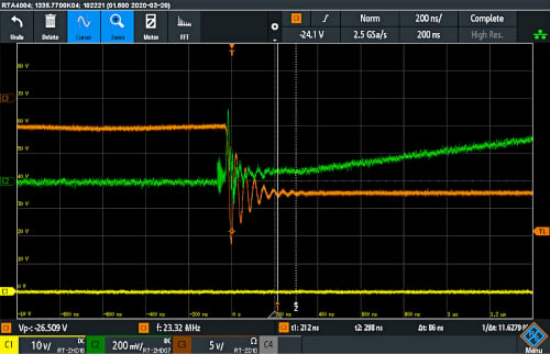
Figure 6. Waveform with calculated snubber values. Image used courtesy of Bodo’s Power Systems
Tips on selecting measurement equipment
Frequency is most easily measured with an oscilloscope, and a low capacitance, high bandwidth probe should be used to avoid affecting the measurement. For work on standard converter types, the R&S RTM3000 or R&S RTA4000 oscilloscopes are a good choice. They provide a measurement bandwidth of up to 1GHz, a power analysis option to automate standard measurements and powerful FFT functionality, which is helpful for general analysis as well as EMI-related debugging.
For more complex converter types like the active clamp flyback converter, a digital trigger system, as available on the R&S RTO6 oscilloscope, is a valuable function. It provides a much higher trigger sensitivity than analog trigger systems found on standard oscilloscopes, in particular if combined with the so-called HD-mode, and allows for complex trigger setups. The HD-mode enhances the vertical measurement resolution and precision by filtering, to give sharper waveforms with details that might otherwise be masked by noise. Advanced triggering is also useful for snubber waveforms that are fast compared with the PWM frequency and may also have intentional jitter, introduced by the PWM controller for EMI mitigation reasons.
Probes are available with a range extending to several GHz bandwidth for transmission-line types, used with a 50-ohm oscilloscope input impedance. When measuring just frequency, the ring waveform can often be observed by simply bringing the tip of a probe close to the circuit without touching, to guarantee no loading.
When amplitude measurements are required to ensure that a semiconductor switch is not stressed, high accuracy is necessary, as safety margins are often small. In many circuits, the voltages are high, approaching the voltage ratings of typical oscilloscope probes, so a good solution is to use a high-voltage differential probe like the R&S RT-ZHD models. For best measurement results, it is important to use them with the short leads delivered, as the probe is specifically compensated for them. The long measurement leads also supplied as a standard accessory can be used if a reduced measurement bandwidth is acceptable, for example when the expected rise times allow limitation of the bandwidth to 5MHz with the integrated lowpass filter in the probe.
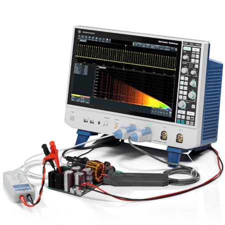
Figure 7. R&S RTO6 oscilloscope with R&S RT-ZHD high-voltage probe and R&S RT-ZC current probe. Image used courtesy of Bodo’s Power Systems
As an alternative to high-voltage differential probes, oscilloscopes are available with isolated inputs with typically 500MHz bandwidth and 1000Vrms input rating.
Further parameters to consider when selecting a high-voltage differential probe are low noise, high linearity, the ability to compensate for a high DC offset and low drift.
Conclusion
Snubber networks are useful tools that that can reduce stress on semiconductors, improve system efficiency and reduce EMI. However, snubber waveforms can be difficult to measure accurately with their high frequency ring often offset from ground by high voltages. Additionally, the trend to faster, wide band-gap semiconductors in silicon carbide and gallium nitride with low device capacitances provides a further measurement challenge with higher frequency ringing. Accurate results can however be achieved by use of suitable probes and probing techniques along with knowledge of potential error sources.
This article originally appeared in Bodo’s Power Systems magazine.
Related Content