Facebook
 Google
 GitHub
 Linkedin
Building a More Efficient DC-DC Converter: Efficiency Evaluation and Loss Analysis of a 300 W Isolated DC-DC Converter
This article focuses on determining the characteristics of the secondary-side MOSFET, necessary for achieving higher efficiency, and examines the direct measurements using the evaluation circuit, comparing them with results from a highly accurate simulation to determine the dominant source of losses.
Efficiency plays a critical role in the design of DC-DC converters, and the power MOSFETs use significantly impacts this efficiency. A specific area with potential for improvement lies in the selection of MOSFETs for the synchronous rectifier on the secondary-side.
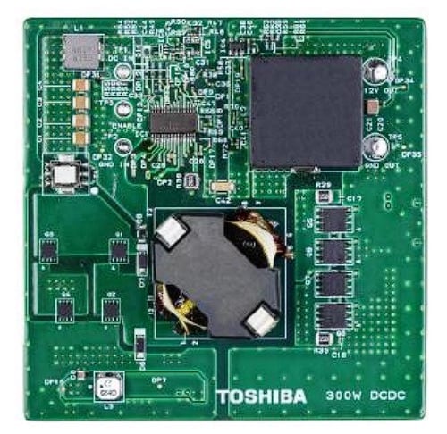
Figure 1. Physical evaluation circuit used to investigate secondary-side losses on a 300 W DC-DC converter.
This article focuses on determining the characteristics of the secondary-side MOSFET necessary for achieving higher efficiency. It studies the direct measurements using the evaluation circuit, as depicted in Figure 1, and, subsequently, compares them with results from a highly accurate simulation to determine the dominant source of losses.
Pursuing Enhanced Efficiency
The quest for higher efficiency dominates most power applications, including DC-DC converters. The definition of efficiency is:
Efficiency = (Vout × Iout) / (Vin × Iin) × 100 [%]
Different design decisions impact efficiency and losses, with a predominant choice being the selection of the primary- and secondary-side MOSFETs, accounting for over 40% of the losses within an isolated DC-DC converter circuit.
Evaluation Board Design
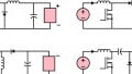
A 300 W DC-DC converter evaluation board was built to gain insight into the losses involved. A simplified circuit diagram is shown in Figure 2.
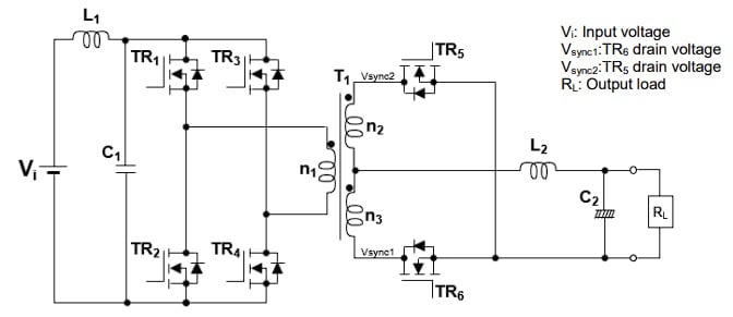
Figure 2. Simplified isolated DC-DC converter circuit.
In this circuit, the primary-side (input side) serves as the input and has two legs and four switching devices (TR1,TR2, TR3, and TR4). The secondary-side (output side) has two devices (TR5 and TR6). These are intended for synchronous rectification. Additionally included is an output smoothing filter with a capacitance of C2 and an inductor of L2. The input voltage is Vi, the output load is RL, and Vsync1 and Vsync2 are the drain voltages for TR6 and TR5, respectively. Observe that TR5 and TR6 have two MOSFETs connected in parallel.
The converter outputs 12 V using a phase-shifted full-bridge (PSFB) topology. The output voltage is regulated by phase-shifted operation between a leg of TR1,TR2, and the leg of TR3, and TR4 with a 50% duty cycle. To prevent shoot-through in the dead time between the high side MOSFET and low side MOSFET, zero voltage switching (ZVS) is achieved to reduce the switching loss of the power converter.
Table 1 shows input and output characteristics of 300 W DC-DC converter.
Table 1. Input and output characteristics of 300 W DC-DC converter.
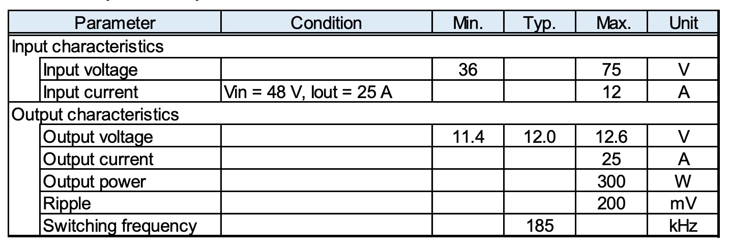
Table 2 summarizes eight operating modes. Figures 3 and 4 illustrate the flow of current in each of these modes using blue and red dotted lines.
Table 2. Operating modes
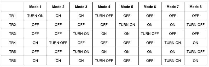
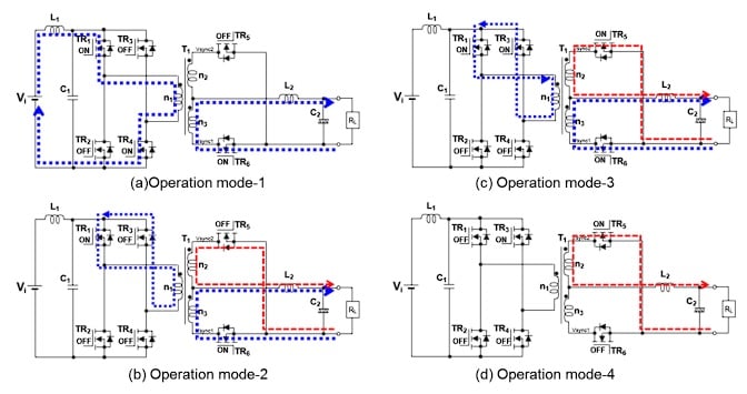
Figure 3. Operating modes 1 - 4.
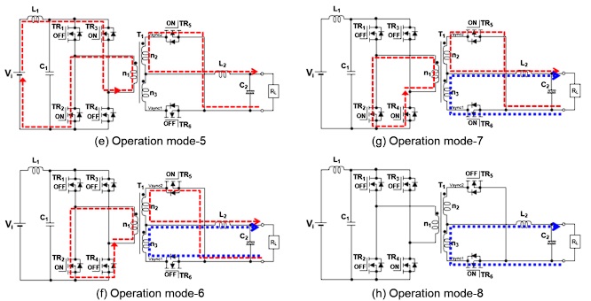
Figure 4. Operating modes 5 - 8.
The waveforms associated with all eight operating modes are summarized in Figure 5. In these simplified waveforms, the following is depicted: gate voltage (VG) and drain current (ID) of the switching devices TR1 to TR6, drain-source voltage (Vsync1, Vsync2) of TR5 and TR6, and voltage between the terminals (VL2) and the current (IL2) of the inductor L2. Recognize that the current through TR5 and TR6 are denoted as negative because current flows from the source to the drain.
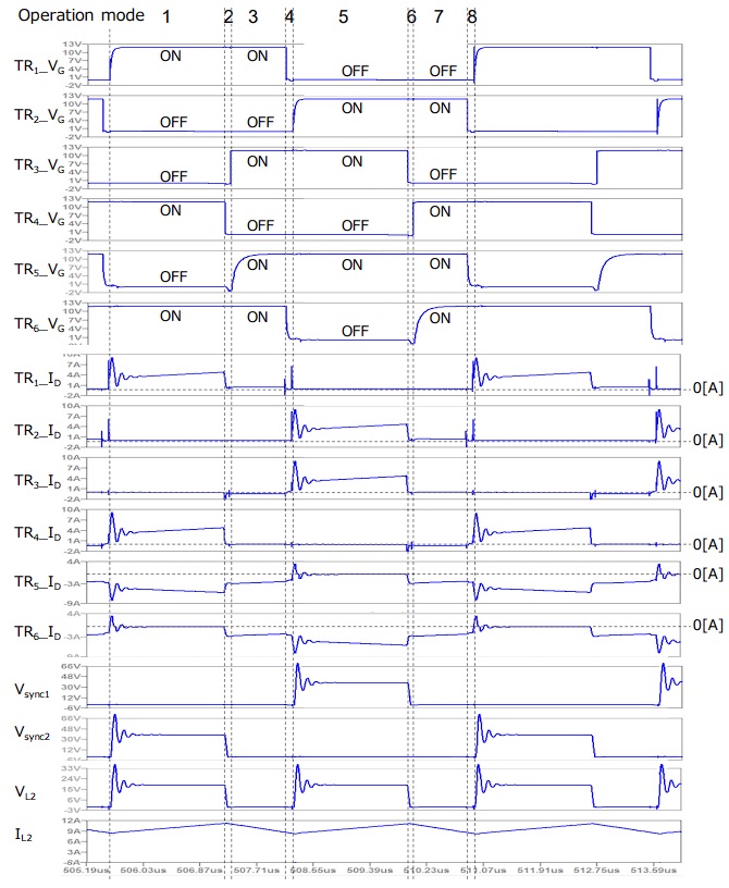
Figure 5. Waveforms associated with all eight operating modes.
Efficiency Evaluation and Loss Analysis
The formula used to calculate efficiency is:
Efficiency = (Vout × Iout) / (Vin × Iin) × 100 [%]
Figure 6 displays the setup for evaluating the efficiency of the 300W isolated DC-DC converter circuit. Vin, Iin, Vout and Iout were measured for two patterns of switching device combinations under these conditions: Vin = 48 V, Vout = 12 V, and Ta (ambient temperature) = 25°C with Iout at 1 A, 3 A, 5 A, 7 A, 10 A, 14 A, 16 A, 18 A, 20 A, and 25 A. The DC-DC converter circuit board is forcibly air-cooled using a cooling fan located near the circuit board.
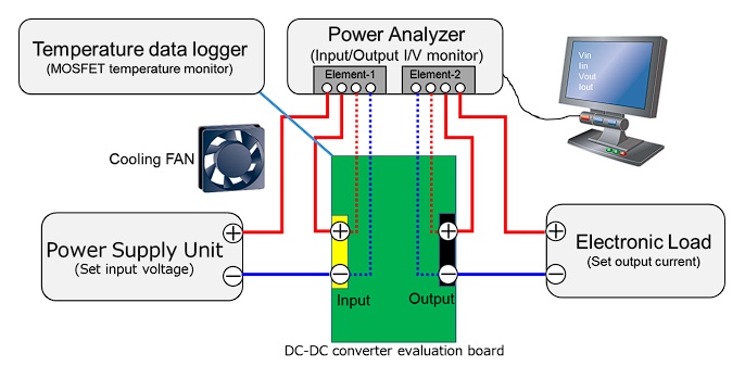
Figure 6. Setup used for efficiency measurement.
This evaluation was performed using the TPN1200APL as the primary-side MOSFET and two different secondary-side MOSFETs (TR5 and TR6): Toshiba TPH2R408QM and an equivalent MOSFET from Company A. All specification details are found on page 9 in the Application Note. The TPH2R408QM MOSFET was selected due to its lower drain-source on-resistance (1.9 mΩ) and lower reverse recovery charge (74 nC) compared to other equivalent products.
Secondary-Side Switching Effect on Power Conversion Efficiency
Figure 7 (a) to (c) compares the efficiency curves using the TPH2R408QM and Company A’s MOSFET. As expected, the TPH2R408QM exhibits the highest efficiency level for medium and heavy loads because conduction loss is the main element of loss in such loads. In addition to this, the TPH2R408QM has a smaller drain-source on-resistance. The maximum efficiency is 94.83% at 16 A of output load and 94.12% at 25 A of full load.
In contrast, the drain-source on-resistance of Company A’s MOSFET is approximately 16% larger than the TPH2R408QM, with efficiencies of 94.65% at 16 A of output load and 93.89% at 25 A of full load.
Figure 8 illustrates the relationship between device temperature and output current for both types of MOSFETs. Notably, the TPH2R408QM exhibits temperatures consistently lower than 45°C, indicating less heat generation than the MOSFET manufactured by Company A.
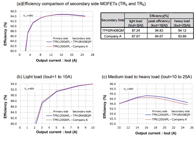
Figure 7. Efficiency curves.
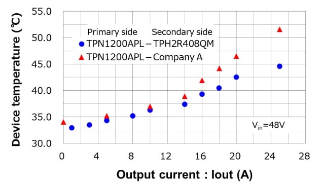
Figure 8. Temperature comparisons.
Loss Analysis Simulation
Loss analysis was performed using a simulator circuit with a high-accuracy device model specifically designed for loss analysis. The evaluation board uses a phase-shifted full-bridge PWM controller IC, but this simulation circuit uses the alternative control model making feedback according to the voltage and current sensing. The simulation circuit is found in Figure 9. The transformer and reactors are based on measurement results. Additional details on simulation design are found in the Application Note.
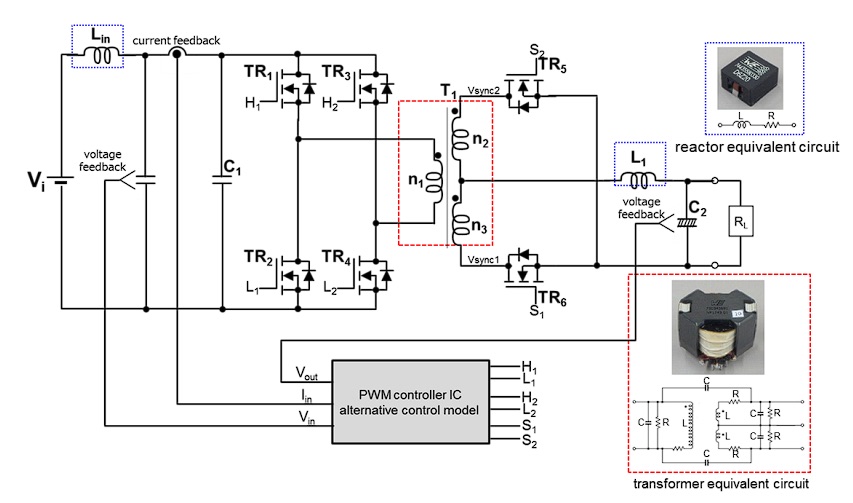
Figure 9. Loss analysis circuit.
After the simulation was verified, results related to loss definition of the secondary MOSFETs were performed. Figure 10 shows how I and V are defined, the timing chart of the secondary MOSFET, and how each form of loss is calculated based on the timing chart. Each loss section is based on a segment of time and six types of losses were calculated.
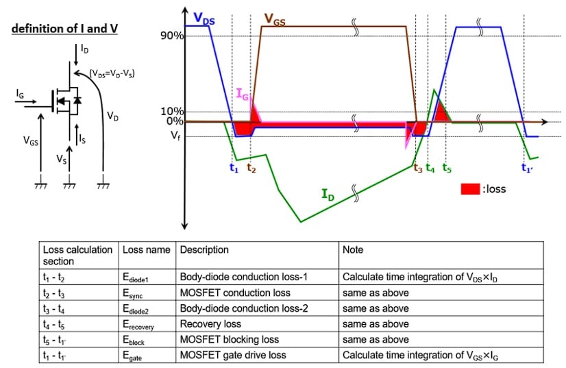
Figure 10. Timing chart for loss calculation.
Which MOSFET Is Best?
The results of loss analysis for the secondary MOSFETs, in the case of TPH2R408QM, are plotted in Figure 11. The dominant form of loss is the recovery loss of the body diodes (which is not sensitive to current) and the conduction loss (Esync), which increases with output current. This indicates that a MOSFET with a low recovery charge and low drain-source on-resistance is the most efficient choice.
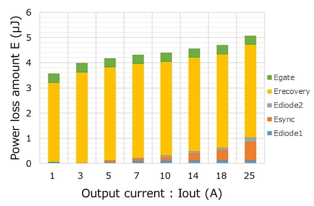
Figure 11. Secondary-side MOSFET loss analysis results grouped by type of loss.
Optimize Efficiency: Explore Secondary-Side MOSFETs
The selection of secondary-side MOSFET for isolated DC-DC converter circuits is vital to overall efficiency. Toshiba offers a robust lineup of power MOSFETs, encompassing a wide range of VDSS from 30 V to 250 V and various drain-source on-resistance types within each VDSS class. Learn more about designing high-efficiency DC-DC converters with Toshiba’s low recovery charge and low drain-source on-resistance MOSFETs with the Reference Design Materials guide.