Facebook
 Google
 GitHub
 Linkedin
Fabricating Different Types of Photovoltaic Cells
The manufacture of crystalline silicon modules involves fabricating silicon wafers, transforming the wafers into cells, and assembling cells into modules.
A wafer is a thin, flat disk or rectangle of base semiconductor material. Wafers are 180μm to 350μm thick and are made from p-type silicon. Crystalline silicon cell wafers are formed in three primary types: monocrystalline, polycrystalline, and ribbon silicon. Each type has advantages and disadvantages in terms of efficiency, manufacturing, and costs.
Monocrystalline Silicon
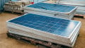
A silicon wafer made from a single silicon crystal grown in the shape of a cylindrical ingot is defined as a monocrystalline wafer (see figure 1). In a crucible, chunks of extremely pure polysilicon are melted with boron. A small seed crystal is slowly rotated in the molten bath and withdrawn. The seed crystal develops into a massive cylindrical crystal up to 40 inches in length and 8 inches in diameter over the course of several hours. Since the ingot is round, the edges are usually cropped to a more rectangular or square shape, allowing cells to be packed more closely in a module. Diamond wire saws are then used to cut individual wafers from the ingot. Commercial monocrystalline cells have efficiencies ranging from 15% to 18%, with certain laboratory samples achieving efficiencies as high as about 27%.

Figure 1. Monocrystalline silicon wafers are sawn from grown cylindrical ingots. Image courtesy of Heng Xing Technology Co. Ltd
Polycrystalline Silicon
A polycrystalline wafer is a silicon wafer made from a cast silicon ingot containing many silicon crystals(see figure 2). To form an ingot, molten silicon is poured into a crucible and cooled steadily and cautiously for several hours. Several silicon crystals form and grow as the molten material solidifies during cooling. The cast ingot is then cut into square or rectangular wafers using wire saws. Polycrystalline wafers can be differentiated from monocrystalline wafers by their square corners and the presence of grain boundaries on the wafer surface. Although polycrystalline cells have marginally lower efficiencies (11.5%–14%) than monocrystalline cells, their lower processing costs and denser packing in modules make them economically competitive with monocrystalline modules.

Figure 2. Polycrystalline silicon wafers are sawn from cast rectangular ingots.
Ribbon Silicon
A ribbon wafer is a silicon wafer made by drawing a thin strip from a molten silicon mixture. The melted material is pulled between parallel dies where it cools and solidifies to form a continuous multicrystalline ribbon. The ribbon is then cut at specific intervals to form rectangular-shaped wafers. While cells produced from ribbon silicon wafers have slightly lower efficiencies (11% to 13%) than other silicon cells, this process is less expensive because there is less material waste, and it does not require ingot sawing.
Cell Fabrication
To convert a crystalline silicon wafer into a functional PV cell, it must undergo additional processing (see figure 3). The wafers are first etched and imperfections introduced during the sawing process are removed by dipping them in a sodium hydroxide solution. The textured surface increases surface area, improves adhesion of subsequent coatings and reduces reflected sunlight.

Figure 3. Several steps are involved in turning silicon wafers into PV cells.
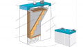
After cleaning, the wafers are mounted on racks and placed in a diffusion furnace, where phosphorus gas penetrates the cell's outer surfaces, forming a thin n-type semiconductor layer that surrounds the original p-type semiconductor material (Figures 3 and 4). The wafer's edge is then abraded to eliminate the n-type material.

Figure 4. The diffusion of phosphorus gas results in the creation of a thin n-type semiconductor layer covering the entire surface of a p-type wafer.
Antireflective coatings are then added to the cell's top surface to minimize reflected light even further and boost cell efficiency. Following the drying of the coatings, grid patterns are screen printed with silver paste on the cell's top surface to provide a point for electron collection and electrical connection to other cells. In general, these grid lines contain two or more main strips throughout the cell, with fine lines originating from the main strips across the cell surface. The arrangement of these grid patterns is a crucial part of cell design since they must be of appropriate size and distribution to effectively capture and conduct current away from the cell, but they must be minimized to prevent covering most of the cell surface, which decreases the cell's effective surface area exposed to sunlight. Finally, a thin layer of metal, usually aluminum, is applied to the cell's entire back surface, which alloys with the silicon and neutralizes the n-type semiconductor layer. This results in the cell's bottom surface being the positive connection, whereas the top surface is negative (see figure 5).

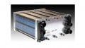
Figure 5. The different materials, processes, and manufacturing steps produce a range of PV cell types.
After cells are produced, each is electrically tested under simulated sunlight and sorted according to its current output. This sorting process largely eliminates problems with the current mismatch among series-connected cells and allows manufacturers to produce modules that are of the same physical size but have different power ratings.