Facebook
 Google
 GitHub
 Linkedin
Packages for the Highest Voltage Class Si IGBTs and SiC MOSFETs
HV LinPak is a new package that adds to several options converter designers have for using Si IGBTs and SiC MOSFETs with nominal blocking voltages above 3.3 kV. It brings to the high-voltage range the advantages demonstrated by its LV variant, such as low stray inductance, paralleling performance, high power density, and the ideal distribution of power and auxiliary terminals.
As electricity increasingly becomes the lifeblood of modern society, so does the importance of power electronics and their efficiency. To minimize energy loss in power electronics, we need to more closely examine all aspects of the components involved.
For the topologies used in these power electronics systems, from classic two-level converters to more advanced 3L NPC with passive or active control or T type to more complex converters like Modular Multi-level or Cascaded H-Bridge Multi-level, there are numerous optimizations for efficiency, component count, harmonic distortion, reliability, and cost. Of all the components used in a power electronics system, the switches used to turn on and turn off the current are some of the most important.
In the very high-voltage switches range (>3 kV), we have observed an aggregation of available options in recent years. On one hand, we have current-controlled devices like Phase Control Thyristors (PCTs) [1] or Integrated Gate-Commutated Thyristors (IGCTs) [2], and on the other hand, voltage-controlled switches like Insulated Gate Bipolar Transistors (IGBTs) or SiC Metal Oxide Semiconductor Field Effect Transistors (MOSFETs).
There are two main classes of packages available for these switches: press-pack solutions (i.e., Hockey Pack for BiPolar and StakPak for IGBT [3]) and isolated modules. For isolated, high-voltage modules, HiPak has been the workhorse of the industry [4]. It is intensively used in traction converters, medium voltage drives, and grid applications (i.e., SVC, interties, STATCOMs, HVDC valves, etc.). More recently, a new package has been proposed [5], and at Hitachi Energy, this package is called LinPak. We launched the first LV LinPak version (Viso=6 kV) for commercial operation in early 2016 [6]. The HV LinPak (Viso=10.2kV) has now come to market (see Figure 1). Acceptance for these packages has been immediate, and demand for them has been widespread due to their improved performance characteristics.
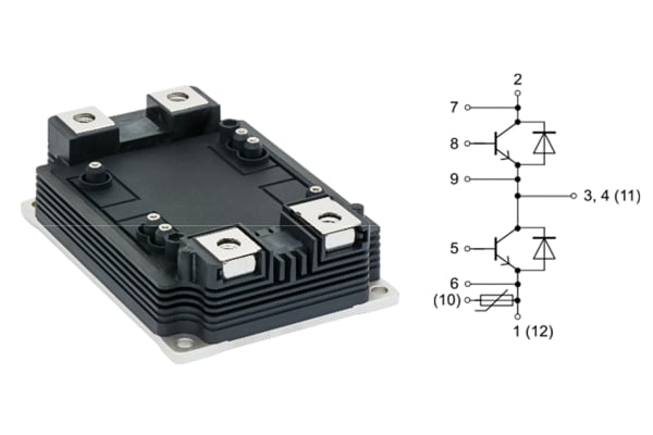
Figure 1. The HV LinPak module. Image used courtesy of Bodo’s Power Systems [PDF]
HV LinPak Features
HV LinPak is designed on the same principles as the LV version. It is a dual (or phase leg) module, with the main power terminals on each side of a long axis. This allows the convenient placement of the gate unit in the middle of the module without any constraints on the busbar design. Moreover, the DC+ and DC- terminals are fed into the module in a co-planar geometry to achieve the lowest commutation inductance. Special care in the design of the module was taken so that the paralleling of these modules can be done with minimal or no current de-rating [7]. In addition to all these improved characteristics, the HV LinPak is available with an optional NTC thermistor, the first module in its class with this option. The following variants for Si IGBT HV LinPak are in development: 3.3 kV 600 A, 4.5 kV 450 A, and 6.5 kV 300 A. Equivalent ratings with SiC MOSFET are in development as well.
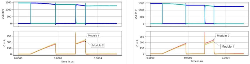
Figure 2. High side (left) and low side (right) double pulse switching curves of two 3.3kV 600A HV LinPak modules in parallel. Image used courtesy of Bodo’s Power Systems [PDF]
Parallel Operation
We have created a setup for testing the HV LinPak in parallel, in accordance with existing literature recommendations [8]. We started the paralleling tests with the 3.3 kV 600 A HV LinPak modules and observed very good current sharing between modules taken randomly from our production (see Figure 2). The position of the modules in the test setup was the most important factor in determining current asymmetries. We obtained the same variance even when we swapped the modules used in the test. The variation of the module parameters (VCEsat, VF, Vth, td(on/off), ..) was representative of the typical distribution of these parameters.
Additionally, we noted a difference in the parallel switching behavior of the high side versus the low side. We saw a big impact on this imbalance when we altered the test setup, i.e., connecting or disconnecting a circuit breaker. Moreover, this difference is, as previously stated, position-dependent and does not change when exchanging or swapping modules.
NTC Option
To enhance the features of this module for the high voltage range, an NTC thermistor is now available as an optional feature. The NTC sensor is mounted on the same substrate as the semiconductor chips, which ensures that the temperature readings are as close as possible to the chip temperature. This enables customers to further optimize the use of the module by reducing the design margins. For instance, when a high temperature is detected, the switching frequency can be temporarily changed to reduce switching losses. Furthermore, if only one module is experiencing increased temperature, condition monitoring management can be applied to avoid a catastrophic failure. Such information would not be available if only the temperature of the cooling water, or a sensor on the heat sink, was used as the trigger.
In Figure 3, we see the voltage signal that was measured over the NTC. We applied a voltage divider technique that is common for such measurement, where we have a resistor (820 Ohm) in series with the NTC thermistor. We see that the NTC sensor is following the temperature of the main substrate on which it is mounted, and the signal has some coupling with the emitter dv/dt. It is important to understand this behavior in order to avoid a false reading. A higher temperature implies a lower resistance, which in turn means a lower voltage drop over the NTC.
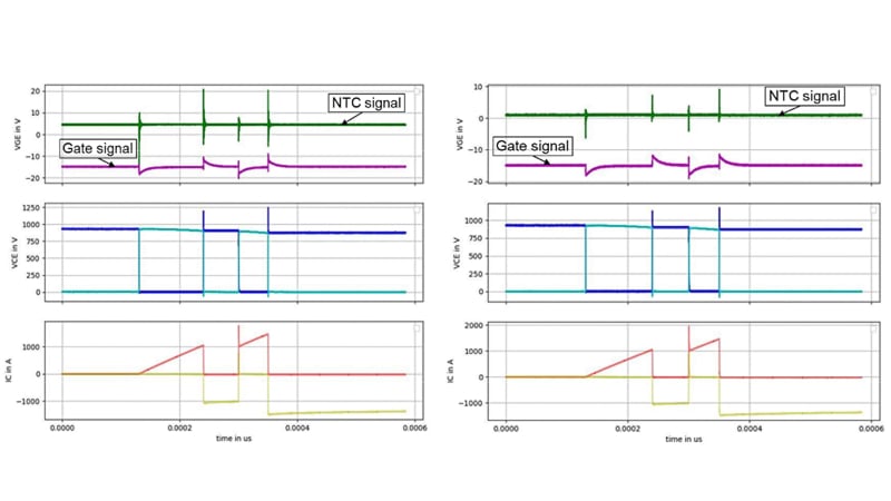
Figure 3. NTC signal curves measured at RT (left) and 150°C (right) of the HV LinPak, assessed with high current switching during a double pulse test. Image used courtesy of Bodo’s Power Systems [PDF]
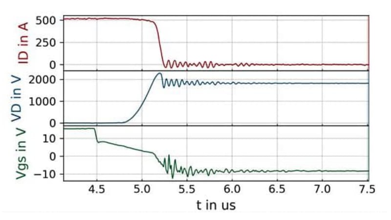
Figure 4. Turn-off of a SiC 500 A 3.3 kV HV LinPak module, 25°C, Rg=3.3Ohm. Image used courtesy of Bodo’s Power Systems [PDF]
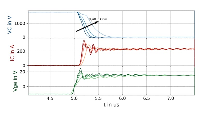
Figure 5. Scanning of Rg for the turn-on of a 3.3 kV SiC on substrate level (Inom=225A), 25°C. Image used courtesy of Bodo’s Power Systems [PDF]
HV LinPak With SiC MOSFETs
Due to its low stray inductance, the HV LinPak can also be equipped with fast-switching SiC MOSFETs. In our improved version of this package, we decreased the internal inductance to ca. 23nH, which enables the device to switch much faster. In this way, the very low switching losses of the SiC devices can be fully utilized. Not only is the internal inductance lower but the substrate design is optimized to ensure that each SiC device experiences the same commutation inductance and the same gate inductance and that the coupling is very homogenous. To ensure a good balance between the two substrates inside the module, we equip each of them with its own gate resistor.
Figure 4 demonstrates the switching waveforms of a 500 A 3.3 kV SiC LinPak. Our target was to have very good controllability, i.e., to be able to vary the switching speed by applying different values for the Rg. It can be seen from the wave curves that good switching is achieved even with external Rg=0 Ohm (see Figure 5). When going from a value of Rg of 0 Ohm to 5 Ohm/ substrate, the di/dt is slowed down from 3.5 kA/us to 1.2 kA/us. The same was observed in the turn-off curves, where the dv/dt was reduced by ca. factor 3 when increasing the Rg from 0 Ohm to 5 Ohm/ substrate. This gives a converter designer the flexibility to choose the gate resistor value that offers the optimal compromise between losses and di/dt or dv/dt constraints.
Conclusions
This article has shown the newest available module for designers of medium voltage converters in applications like traction, industrial drives, frequency converters for grid applications, and many others. With state-of-the-art characteristics like low stray inductance, high current density, optional NTC thermistor, optimal electric design for paralleling, and optimal mechanical design for compact inverter design, the HV LinPak has established itself as the new industry standard.
References
[1] V. Botan, J. Waldmeyer, M. Kunow, K. Akuratti, “Six Inch Thyristors for UHVDC Transmission”, Proc. PCIM 2009
[2] T. Wikstroem, U. Vemulapati, B. Oedegard, “A 4.5kV RC-IGCT with Diode Segmentation for MMC Inverters”, Proc. PCIM 2022
[3] B. Boksteen, D. Prindle, F. Dugal, W.A. Vitale, E. Tsyplakov, V. Botan, G. Pâques, “Second generation BIGT chip advancing the StakPak platform”, Proc. PCIM 2020
[4] V. Botan, D. Schneider, “A journey from one to a million HiPaks”, Bodo’s Power Systems, May 2020
[5] T. Wiik et al., Roll2Rail, D1.2 “New generation power semiconductor – Common specification for traction and market analysis, technology roadmap, and value cost prediction”, 2016
[6] R. Schnell, et al., “LinPak, a new low inductive phase leg IGBT module with easy paralleling for high power density converter designs”, Proc. PCIM 2015
[7] R. Ehrbar, G. Salvatore, A. Rosch, A. Baschnagel, A. Ruiz1, W. Vitale, V. Sundaramoorthy, F. Fischer, V. Botan, G. Pâques, “HV LinPak - A high voltage half bridge IGBT power module with balanced switching behavior for easy paralleling”, Proc. PCIM 2022
[8] J. Weigel, J. Boehmer, E. Wahl, A. Nagel, E. Krafft, “Paralleling of high power dual modules: Standard building block design for evaluation of module related current mismatch” 2018 (EPE’18 ECCE Europe), P.1–P.10, 2018.
This article originally appeared in Bodo’s Power Systems [PDF] magazine
Featured image used courtesy of Adobe Stock