Facebook
 Google
 GitHub
 Linkedin
Multiply the Power of a Boost Converter with a Versatile Phase Expander
There’s a general understanding in the engineering community that multiphase functionality is required when boost converters must supply high output voltages, work from low input voltages, provide high step-up ratios, or support high load currents. Multiphase boost designs have a number of advantages over single-phase designs, including: increased efficiency, improved transient response, and reduced input and output capacitance values (due to reduced inductor ripple current and ripple current in the input and output capacitors) resulting in reduced thermal stress on the components of the entire boost converter power train.
The easy part of designing a multiphase boost converter is connecting the input supply and output rails to reduce the size and cost of the input/output filters. The difficult part is connecting the outputs of the error amplifiers and feedback pins of the phase controllers to ensure balanced current sharing and correct phase synchronization. Both signals are extremely sensitive to noise and, even with a very careful layout, can be affected by the sharp current and voltage changes typical in boost converter applications. Some boost controllers come with multiphase functionality to solve this problem, but many do not. For controllers that do not have multiphase circuitry included, the LT8551 multiphase boost converter phase expander solves the problem by operating alongside, and detecting the states of, the switching components of the primary controller. The LT8551 duplicates its functionality, measures the primary controller inductor current, and adjusts the inductor current in each added phase. The LT8551 is an excellent choice for automotive and industrial applications due to its high input/output voltage (up to 80 V) and ability to produce very high power boost converters, including those with bidirectional current flow.

Figure 1. The interface of the LT8551 phase expander U1.1 to the primary controller U2. The four additional (expanded) power phases of the solution are shown in Figure 2. Image used courtesy of Bodo’s Power Systems
Functionality of the Converter
Figure 1 and Figure 2 show a complete LT8551-based phase expander solution. To clarify functionality, the phase expander U1 is divided into three subcircuits: U1.1, U1.2, and U1.3. The interface, U1.1, communicates with the primary controller U2 and any external signals. The power stages U1.2 and U1.3 implement actual power conversion and control the MOSFET switches. All three sections of U1 shown in Figure 1 and Figure 2 are integrated in the LT8551 controller.
The primary controller, U2, senses the output voltage through its FB pin. It also completes the functionality of the peak current-mode control with its ITH pin as the output of the error amplifier. All high impedance circuitry (off the FB pin) and noise sensitive components (off the ITH pin) are adjacent to U2 and do not connect to external components. This approach enables compact and noise-shielded layouts.
Instead of using the typical feedback and error amplifier signals to expand phases, the LT8551 implements an elaborate (but more robust) switch state detection scheme. The subcircuit U1.1 relies on the robust signals of the gate drive voltages, BG and TG, and switching node signal, SW, of the primary controller to manage the four phases comprising the power trains driven by U1.2 and U1.3. The controller U1 equally balances the inductor currents among all phases (extender and primary). This is done by measuring the output currents of each channel via the corresponding current sense ISPx, ISNx pins, and the ISP and ISN terminals connected to SENSE+ and SENSE– of U2. The INTVCC and bootstrap voltage (BOOST) signals are also factored into the control equation.

Figure 2. An electrical schematic of the LT8551 power section, U1.2 and U1.3. The LT8551’s interface to the primary boost controller is shown in Figure 1. The VIN = 6 V to 46 V, while the VOUT = 48 V at 30 A. Image used courtesy of Bodo’s Power Systems

Figure 3. Converter efficiency at VIN = 24 V with convection cooling (no air flow). Image used courtesy of Bodo’s Power Systems
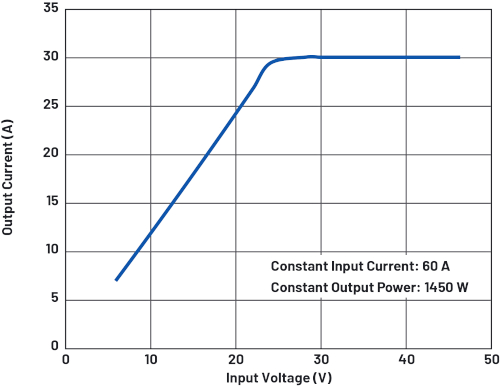
Figure 4. Converter input voltage vs. load current derating curve. Image used courtesy of Bodo’s Power Systems
The schematics in Figure 1 and Figure 2 illustrate a minimum configuration for a boost converter featuring up to five phases. The LT8551 can be used to scale up nearly any single-phase boost controller up to 18 unique phases, with a corresponding multiplication of available output power. In >5-phase configurations, one LT8551 is the master, with additional LT8551 controllers acting as slaves. The CLK1 signal of the master synchronizes primary and slave controllers, whereas the CLK2 signal defines the phase angles for the consequent phases, with up to 18 unique angles. The 18-phase limitation does not necessarily limit the number of channels—if channels are allowed to share the same phase angle, then the number of power phases is essentially unlimited.

Figure 5. An LT8551-based demonstration circuit DC2896A-B. Image used courtesy of Bodo’s Power Systems
The power train configuration shown in Figure 1 and Figure 2 comprises N-channel power MOSFETs Q1 through Q20, inductors L1 through L5, and input and output filters. The efficiency of the converter is shown in Figure 3, with a maximum output current of 30 A, an output voltage VOUT = 48 V, and an input voltage VIN = 24 V. The load current should be reduced to lower than VIN to limit the input current and thermal stress. The load current derating curve is presented in Figure 4. The LT8551 includes internal inductor current balancing circuits that provide excellent current sharing between the phases, from ±6% to ±10% at maximum.
To reduce thermal stress on both controllers, especially at higher voltages, use the auxiliary power source (AUX). One solution can be found in the LT8551’s schematics. A photo of the DC2896A-B evaluation circuit, with designated primary and expanded phases, is shown in Figure 5. The thermal image of the expanded phases is shown in Figure 6.

Figure 6. An LT8551-based demonstration circuit thermal image with convection cooling (no air flow). VIN = 24 V, VOUT = 48 V at 25 A. Image used courtesy of Bodo’s Power Systems
Conclusion
The LT8551 phase expander gives power supply designers a flexible tool to build high power, high efficiency boost converters by expanding switching phases until the desired limit of power is reached. High frequency (up to 1 MHz) helps minimize power components’ size, and integrated gate drivers, along with accurate inductor current monitoring and balancing, help prevent saturation and evenly spread heat across a board’s surface.
About the Author

Victor Khasiev. Image used courtesy of Bodo’s Power Systems
Victor Khasiev is a senior applications engineer at ADI with extensive experience in power electronics both in ac-to-dc and dcto-dc conversion. He holds two patents and has written multiple articles. These articles are related to using ADI semiconductors in automotive and industrial applications. Topics cover step-up, step-down, SEPIC, positive-to-negative, negative-to-negative, flyback, forward converters, and bidirectional backup supplies. His patents include efficient power factor correction solutions and advanced gate drivers. Victor enjoys supporting ADI customers by answering questions about ADI products, designing and verifying power supply schematics, laying out printed circuit boards, and troubleshooting and participating in testing final systems.
This article originally appeared in Bodo’s Power Systems magazine.