Facebook
 Google
 GitHub
 Linkedin
LV100 - a Dual Power Module for the Next Generation Railway Inverters
This article discusses the new standard dual-module package specially developed for High Voltage IGBTs HVIGBTs used in railway applications.
The power module topology is half bridge. The main intention for creating such dual power module is reducing the module’s internal stray inductance. In order to minimize the internal voltage spike – one of the bottlenecks for keeping the RBSOA at maximum inverter output current. Each new chip generation shows increased current switching slope di/dt causing higher overvoltage spikes inside the package if the power module’s stray inductance would be kept constant. The issue becomes even more challenging when wide band gap semiconductors are used, because the switching speed can be increased by a factor of ten compared to today’s Si-IGBTs. As first step MITSUBISHI ELECTRIC is going to introduce power modules in LV100 package with Si- and SiC- chips having a blocking voltage capability of 3300V. As second step the LV100 package will be applied to 1700V chips.
General advantages of the new package design
The general motivation for developing of LV100 was strong requirements from European Market for propulsion inverters which were concluded in the deliverables of Roll2Rail community [1]. Besides decreasing the stray inductance the scalability is on focus of requested features. The decrease of stray inductance to 10nH is forced by the continuous increase of switching speed and introduction of wide band gap semiconductor materials. The scalability is a feature simplifying logistic, costs and availability of propulsion inverter.
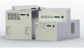
Mitsubishi Electric uses the possibility of setting new standard traction power module by introducing of superior and proved technologies. The output power corresponded to the output current is going to be increased by introducing of next chip generation and semiconductor materials. One of the bottlenecks for increasing the output power is not related to semiconductor performance, it is about the current handling capability of main terminals [2]. This technology evolution is respected by designing three paralleled AC power terminals in LV100- package instead of two as proposed by other dual-module concepts (see Fig.1). The design of auxiliary terminal arrangement satisfies the pollution degree 3 requirements [3]. The height of auxiliary terminals is 5mm in order to use double-layer PCB for gate driver. The chip set used in the Si-based LV100 module is belonging to the X-series [4] [15], and corresponds to the latest 7th generation Si-chip technology. The chipset used in the SiC-based LV100 module was already proved in the field operation test, in the famous Japanese high speed train Shinkansen [5]. The chips use SCC technology for further decreasing the humidity impact on reliability [6]. The innovative baseplate design is focusing on increasing the lifetime expectation and reducing thermal stress on semiconductors [7].

Figure 1: The housing of LV100 power module
Baseplate
Special attention was paid on innovation provided by advanced baseplate. For the first time the material of baseplate will be not based on metal matrix composite AlSiC, the used standard material today for railway application. Mitsubishi Electric is going to introduce Al with following advantages vs. AlSiC. The advantage of Al is thermal resistance which is lower vs. AlSiC [8, 9]. Additionally the weight of Al baseplate is lower forwarding the advantages to the railway equipment, increasing indirectly energy efficiency.
Historically Mitsubishi Electric uses AlN as insulating ceramic layer in power modules. This material provides 7 times higher thermal conductivity compared to the second popular insulation material Al2O3. The using of Al was inhibited in the past by mismatching of thermal expansion coefficients CET. Due to this mismatch the solder layer between baseplate and ceramic insulator is stressed under cyclic load conditions and limits the lifetime of power module. In LV100 this bottle neck, the solder between ceramic and baseplate, is completely eliminated by newly available Metal Casting direct Bonding MCB technology [7]. The thermal stability of Al baseplate is additionally supported by AlN strips implemented into the baseplate. This proven technology was applied for the first time to high power semiconductor modules about 7 years ago, when Mitsubishi Electric started the manufacturing of Mega Power Dual Modules CM1800DY-34S and CM2500DY-24S. Besides the drastically increased thermal cycling capability the elimination of substrate solder layer provides the additional effect of reduced thermal resistance Rth(j-c) by approximately 25%.
In high power modules with conventionally soldered ceramic substrates the reachable power chip density is limited by the insulation material geometry. The new MCB baseplate structure is removing this limitation and allows to enlarge the insulation surface and to optimize the chips location.
Finally MCB and Al material allow an improved baseplate flatness control. The baseplate flatness is reduced to 33um which contributes to the reducing of thermal grease thickness. The total advantage of improved baseplate results in a reduced contact thermal resistance between baseplate and heat sink by 30% [7].
As summary the advanced baseplate reduces the weight, increases the output power and increases the life time capability of LV100 power module.

Figure 2: The MCB baseplate with flatness reduced to 33um

Figure 3: Improved baseplate results in a reduced contact thermal resistance
X-Series chip set
The X-series chip set was developed by Mitsubishi Electric in order to satisfy the current and future market requirements for high efficiency, high junction and operation temperatures, increased rated current, increased RBSOA, RRSOA, SCSOA and improved robustness against humidity.
The efficiency is increased by the introduction of trench-gate structure. The increasing of operation temperature is achieved by optimization of N buffer layer and by gettering [4]. With these methods the leakage current at Tj=150°C is low and does not exceed the values that the previous chip generation was showing at Tj=125°C. The implemented chip structure is given in Figure 4. The additional effect of advanced gettering process is significantly increasing of cosmic ray withstand capability [10]. The Long Term DC Stability LTDS affected by cosmic ray becomes nowadays one of the key criteria for selecting the appropriate power semiconductor for railway applications. Special engineering focus was done on humidity resistance due to increased awareness of Roll2Rail and power electronics communities on reliability impact of environmental conditions [11][14]. The introduced Surface Charge Control SCC technology prevents formation and polarization of outer surface charges QSS [6] that may disturb the electrical field distribution in the chip’s guard ring area.

Figure 4: Chip structure
Switching Performance
The standard switching tests of CM450DA-66X are performed under consideration of rated values and two different junction temperatures. The results are shown in figures 8 and 9. The contribution of low stray inductance is visible. The di/dt and dv/dt values are indicated in order to estimate the EMC level. The well balanced triangle trade-off between switching loss, static loss and short circuit robustness of new X-series IGBT-chip was described already in the December 2016 edition of this journal [12].

Figure 5: Motor acceleration mode with power factor 0.9

Figure 6: Braking mode with negative power factor of -0.9
Performance under different application conditions
The performance of CM450DA-66X, the Si based LV100 power module 450A/3300V is presented in figures 5 and6. The X-axis represents the inverter output AC current, the Y-axis represents the PWM switching frequency. The power loss of the module is assumed to be Pv=750W, the value is comfortable for air forced cooling. For liquid cooling systems the above loss figure can be simply doubled. Figure 5 shows the motor acceleration mode with power factor 0.9 and figure 6 shows the braking mode with negative power factor of -0.9. The figures shows similar output power capability in both operation modes which corresponds to the modern railway requirements to acceleration or regenerative energy. The using of braking regenerative energy helps to reduce railway energy consumption. The railway energy saving is one of activities of Mitsubishi Electric keep our tomorrow green [13].

Figure 7: Performance comparison of three types power modules in the same LV100 package
Comparison of Si vs SiC
The tribute to the future, to the use of SiC in next generation power electronic systems, is paid in figure 7. This figure shows a performance comparison of three types power modules in the same LV100 package: (1) Si based (2) Si IGBT and SiC diode hybrid (3) SiC based. The comparison is based on the same application conditions: Vcc=1800V; Ic=450A; fc=0.5kHz, PF=0.85. The Full SiC power module allows to reduce power loss of a module by half compared with Si. Or, taking the advantage of having 3 AC terminals in the LV100 package, the inverter output current could be doubled. The SiC power modules contributes to increasing of switching frequency, to reducing of propulsion motor loss, to increase of power density (compactness) of traction inverters, to increasing of total traction efficiency, to decreasing of Energy Consumption Index ECI.

Figure 8: Turn on losses

Figure 9: Turn off losses
About the Authors
Eugen Stumpf works as the Application Engineering Manager at Mitsubishi Electric Europe B.V, a wholly-owned subsidiary of Mitsubishi Electric Corporation, headquartered in Tokyo, Japan. He earned his Engineering Diploma in Power and Energy at FHD University of Applied Sciences Dusseldorf. He also earned his Master of Business Administration (MBA) at FOM University of Applied Sciences for Economics and Management.
Eugen Wiesner is an Application Engineer at Mitsubishi Electric Europe B.V., Ratingen Germany, one of the branches of the Japanese multinational electronics and electrical equipment company, Mitsubishi Electric Corporation. He earned his Master's of Science in Electrical Engineering at the University of Applied Sciences Dusseldorf located in Germany.
Kenji Hatori works as an Assistant Manager on Project Management at the Mitsubishi Electric Corporation, Fukuoka Japan, a branch of the Japanese multinational electronics and electrical equipment company, Mitsubishi Electric Corporation, that specializes in power device works.
Hitoshi Uemura works at the Mitsubishi Electric Corporation, Fukuoka Japan, a branch of Mitsubishi Electric Corporation which is one of the world's leading names in the manufacture and sales of electrical and electronic products and systems used in a broad range of fields and applications.
Shinichi Iura works at the Mitsubishi Electric Corporation, Fukuoka Japan, a branch of Mitsubishi Electric Corporation which is one of the world's leading names in the manufacture and sales of electrical and electronic products and systems used in a broad range of fields and applications.
Reference
- http://www.roll2rail.eu/
- Krafft et al., “A New Standard IGBT Housing for High-Power Converters”. EPE 2015, Geneva, Switzerland
- EN50124. “Railway applications Insulation Coordination”. European Standard, April 2006
- Tanaka et al., “Durable Design of the New HVIGBT modules”. PCIM 2016, Nuremberg
- Mitsubishi Electric Press Release 2942. “Mitsubishi Electric Installs Railcar Traction System with All-SiC Power Modules on Shinkansen Bullet Trains”. June 25, 2015, Tokyo
- Honda et al., “High Voltage Device Edge Termination for Wide Temperature Range plus Humidity with Surface Charge Control (SCC) Technology”. Proc. ISPSD 2016, Prague, Czech Republic
- Sakai et al., “Power Cycling Time improvement by reducing thermal stress of a new dual HVIGBT module”. EPE 2017, Karlsruhe, 2016
- D.D.L Chung. “Materials for Thermal Conductions”. Applied Thermal Engineering 21, pages 1593-1605, 2001
- Jiang et al., “Advanced Thermal Management Material”. Chapter 8. Springer, New-York, 2013
- Uemura et al., “Optimized Design against Cosmic Ray Failure for HVIGBT Modules”. Proc. PCIM Europe 2011, pages 26-31, Nuremberg, Germany
- C. Zorn, N. Kaminski “Temperature Humidity Bias (THB) Testing on IGBT Module at High Bias Levels”, CIPS2014, Germany, ISBN 978-3-8007-3578-5, 2014
- Wiesner et al., “Line Up Expansion of X-Series High Voltage IGBT Modules in the 3300V Class”. Bodos Power Systems, December 2016, pages 36-37. bodospower.com
- Mitsubishi Electric press release 2732. “Mitsubishi Electric Develops Regenerative Power Optimization Technology for Railway Energy Saving”. February 2013, Tokyo
- N. Tanaka, K. Ota, S. Iura, Y. Kusakabe, K. Nakamura, E. Wiesner, E. Thal “Robust HVIGBT module design against high humidity”, PCIM Europe2015, Germany, p. 368-373, 2015 [15] K. Hatori at al., “Wide Temperature Operation of high isolation HVIGBT”. Proc. PCIM Europe 2010, pages 470-475, Nuremberg, Germany
This article originally appeared in the Bodo’s Power Systems magazine.