Facebook
 Google
 GitHub
 Linkedin
3D Bond Wire Modelling and Electro-Magnetic Simulation Accelerates IGBT Module Development
This article introduces software MFis Wire and its advantages in significantly shortening time for creating complex 3D geometry models of bond wire layouts.
Raffael Schnell and Samuel Hartmann are co-authors of this article originally published in Bodo’s Power Systems magazine.
Speeding up the electromagnetic module design for maximum Chip performance utilization and highest robustness with the latest tools for bond wire routing and electromagnetic simulations.
Creating Bond Wire Layouts Using 3D CAD
Although 3D CAD systems today are well established in power module development for virtual prototyping and creation of the necessary product documentation, the bond wires are often missing in 3D models. While a single bond wire can be modeled with some arcs and lines, modeling a whole bond wire layout is time-consuming, since often each bond wire has its individual geometry. To fill this gap, the first version of the software MFis Wire was released in 2020 by MFis GmbH, a company providing engineering services and tools with a focus on power electronics packaging.
MFis Wire provides a user-friendly interface (see figure 1) and makes 3D modeling of wedge, ribbon, and ball bond wires fast. A bond wire is drawn by selecting the start and endpoint of the wire and interactively defining its loop shape and foot rotation. Many CAD commands like copy, move, mirror, array can be used to modify one or more selected bond wires or bond points for example for adjusting the pitch of a row of bond wires.

Figure 1: The software MFis Wire, used for drafting the bond wire layout of the ED-type power module
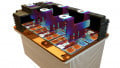
The software has been realized as a plug-in for the powerful and affordable Rhino3D CAD platform. For the creation of bond wire layouts, only basic skills of CAD modeling are needed. Short training videos showing the workflow guide the user to create first wire layouts within short time. Once a 3D model is ready, it can be exported to many industry-standard CAD formats or converted to a 2D drawing with bond point coordinates. Since Rhino3D has powerful rendering features, photo-realistic images of a power module layout are created with low effort (see figure 4).
Geometry Optimization for Fast Parasitic Extraction
A 3D bond wire layout geometry can for example be used for documentation, electro-thermal finite element analysis or parasitic extraction purposes. Depending on the targeted use, the wire cross-sectional geometry must be chosen differently. For documentation purposes, a circular cross-section looks most natural and has lowest file size.
When targeting electro-thermal finite element analysis, only the cross-sectional area of a wire is of relevance. The best choice is a triangular cross-section with the same cross-sectional area as the original wire, which makes the geometry efficient for meshing and computation and will not influence the bond wire temperatures and resistances obtained as a result from the finite element analysis.
For parasitic extraction, the cross-sectional shape is relevant. If a circular cross-section is used, the mesher of the parasitic extractor will approximate the round shape with several elements. Typically, a better trade-off between computing time and accuracy is achieved when the approximation is already implemented in the input geometry. Good results are obtained using a hexagonal wire cross-section.
Bond wire geometry modeling and parasitic extraction were done for the ED-type module with a bond wire layout consisting of 165 wires, many of them having their individual shape. After having created the wire layout, that connects 661 points, the wires were exported in variants with circular and hexagonal cross-sections and processed using the parasitic extractor Ansys Q3D. Figure 2 shows the difference in mesh obtained for the variants with circular and hexagonal cross-sections. For the wire with a circular cross-section, the mesher puts a lot of triangular cells to approximate the round shape, which resulted in the most realistic results but needed 5.5 hours to converge in contrast to only 71 minutes in case of the geometry with hexagonal cross-section. Also, the memory consumption of 22.3 GB was much higher for circular wires than 11.4 GB for hexagonal wires. The difference in the obtained module self-inductance was only 0.1%.
ED-Type Module Design Optimization
As an emerging company, it is crucial for SwissSEM Technologies AG to bring its first products to the market in high quality and short time. Electromagnetic and thermal optimization are essential for excellent device performance. The ED-Type, an industry-standard 17 mm height 62 x 152 mm IGBT module, offers special challenges for internal current sharing between the IGBTs due to its longish design. Most classic layouts suffer more or less current imbalance between the chips, and it is our goal to launch a module with the best possible current homogeneity in order to have the full benefit of our latest IGBT i20 generation.
With the help of the MFis Wire software, we were able to quickly generate various design variants including variations in the bond wire layout. This enabled us to simulate the electromagnetic couplings of the variants in Q3D and make switching simulations with the SIMetrix Spice simulator using the extracted circuit models from Q3D. These simulations were the basis for a better understanding of the device and its internal couplings. Especially as already small variations of the wire position and shape in the mm range can have a significant impact on the coupling. Hence a simplified geometry, as it would be obtained when using the wire tool available in Q3D, is not sufficient. Together with heat-transfer simulations, an optimized layout was found. From a thermal resistance point of view, both variants of chip positioning offer the same Rth. However, the “Layout straight” offers more potential to improve the current sharing compared to the “Layout classic”, especially to slow down IGBT #3 which is closest to the common power emitter connection (see figure 3). For the final layout optimization, the gate position of IGBT #3 was rotated and the main emitter wire and gate wire layout was optimized (see figure 4). As a result, the current imbalance was reduced from 30% of the “Classic layout” to 17% of the “Layout straight optimized”. This is a significant step that improves the load balancing within the IGBTs, but as well yields in a higher safe operating area utilization of the IGBT chips.

Figure 2: Mesh created by Ansys Q3D for bond wires with circular and hexagonal cross sections

Figure 3: Comparison of current sharing with different layouts and thermal reference

Figure 4: Layout straight (left) – Layout straight optimized (right)
Conclusion
Today’s simulation tools for thermal as well as electromagnetic simulations are very powerful, shorten development time and improve the quality of IGBT module designs significantly. Still, the input for the finite element simulations needs to be as accurate as possible and reflect the final product design if the optimal result is to be achieved. Especially for complex details like wire bonds, obvious simplifications are attractive at first glance due to the tedious and time-consuming work it requires in the CAD. However, the accuracy of the results will suffer from simplifications, and the full potential of the simulation tools is not utilized.
By using the software MFis Wire, time is significantly shortened for creating complex 3D geometry models of bond wire layouts. Using hexagonal wire cross-section in the input geometry of the parasitic extractor results in four times faster computation, which makes it possible to investigate several layout variants in a single workday. This method used at SwissSEM, enabled an improvement of the ED-Type module’s internal current sharing by nearly a factor of two compared to classic design approaches.
About the Authors
Raffael Schnell is now the Vice President for Product Management and Application at SwissSEM Technologies AG. He has more than 25 years of experience in the power semiconductor industry in the areas of Product Management, Development, Testing and Application of power semiconductors. He earned his Electronics Engineer diploma at Lernzentren (Learning Center) Baden. He also received his Diploma in Energy Technician HF, and Energy Technology at ABB Technical School, Baden, Switzerland.
Samuel Hartmann has been with ABB Switzerland Ltd., Semiconductors, Lenzburg, Switzerland, as a Principal Engineer, where he was involved in the development of IGBT power module technology and products. In 2019 he founded MFis GmbH which is offering engineering tools and services for power electronics devices. He earned his Masters in Science degree in Physics from the Swiss Federal Institute of Technology, Zurich, Switzerland.
This article originally appeared in Bodo’s Power Systems magazine.