Facebook
 Google
 GitHub
 Linkedin
SiC-MPS Diodes Under Stress: Robust Performance Under Extreme Conditions
What is the reverse recovery behavior of SiC-MPS diodes in scenarios that challenge their thermal and dynamic robustness? This article provides a closer look.
Article co-authored by Zhe Yu and Bengt Sprätz, both Nexperia, Hamburg/Germany.
This article is published by EEPower as part of an exclusive digital content partnership with Bodo’s Power Systems.
Power electronic systems, such as on-board chargers (OBCs) and insulated DC/DC converters, impose stringent requirements on component reliability, particularly under thermal and electrical stress. SiC-Merged-PiN-Schottky (MPS) diodes, which combine the characteristics of a Schottky barrier and a P-N junction, offer significant advantages in terms of both switching performance and robustness [1].
This study explores the reverse recovery behavior of various SiC-MPS diodes from Nexperia in scenarios that challenge their thermal and dynamic robustness. The primary objective is to assess their performance limits and evaluate their suitability for demanding industrial applications.

Image used courtesy of Adobe Stock
Test Concept & Measurement Conditions
Double-pulse tests were carried out on Nexperia’s 650 V SiC-MPS diodes [2] with nominal current ratings (IN) of 6 A, 10 A, 16 A, and 20 A. The applied stress conditions included forward conducting currents of up to 120 A and case temperatures up to 175 °C, representing a challenging operating regime for the devices under test. The test samples covered a broad range of package types, including wire-bonded TO247, TO220, DPAK and D2PAK (e.g. PSC1065J) as well as innovative clip-bonded variants such as CFP40 and CFP60.
In order to evaluate the impact of switching speed on device robustness, the diode turn-off current slope (di F/dt) was increased up to approximately 9 A/ns. These test conditions were chosen to emulate realistic worst-case scenarios in power electronic systems, particularly under transient overcurrent and thermal stress, enabling a reliable assessment of the diodes’ reverse recovery behavior.
The reverse recovery charge Qrr, used as a key parameter for characterizing reverse behavior, was determined according to equation (1), in which the parameter iF equals the diode forward current [3].
\[Qrr = \int^{t_{1}}_{t_{0}}(-i_{F})dt\,\,\,\,\,\,\,\,\,\,(1)\]
Here, t0 denotes the time of the first zero-crossing of the forward current iF, and t1 is defined as a steady-state point in time after the completion of the switching transition.
Measurement Results & Observations
Figure 1 illustrates the reverse recovery charge Qrr as a function of diode turn-off current for a commutation speed of up to 4 A/ns and a case temperature of 175 °C. The measurements were conducted on D2PAK-packaged SiC-MPS diodes with nominal current ratings of 10 A, 16 A, and 20 A. All devices are based on the same die technology but differ in die size, with the 20A-die featuring the largest active area.
Up to a certain current threshold, Qrr remains nearly constant, even at elevated temperatures of 175 °C, as shown in Figure 1. Until this threshold, the reverse recovery appears to be primarily influenced by capacitive effects, where against bipolar carrier injection playing only a minor role.
This corresponds to a nearly idealized unipolar condition, where the reverse recovery charge is dominated by the junction capacitance, which can be approximated by:
\[Q_{c}-\int C(V)dV+Q_{0}\,\,\,\,\,\,\,\,\,\,(2)\]
Assuming the diode capacitance is unaffected by commutation, temperature, or other dynamic effects, equation (2) describes a charge primarily influenced by the blocking voltage. Here, Q0 represents an integration constant. Moreover, equation (2) implies that the capacitive charge Qc and thus Qrr in this operating range, scales with the die area.
A clear influence of die size is also visible in Figure 1. Due to their smaller active area, devices with smaller dies exhibit reduced parasitic capacitances, which leads to lower Qrr values. This effect becomes particularly apparent at a forward current of 10 A (IF = 10 A), where the 10A-die shows the lowest reverse recovery charge.
However, these smaller dies also demonstrate increased sensitivity to temperature. The temperature-induced rise in Qrr begins at significantly lower forward current levels compared to devices with larger die areas. For instance, the 10A-die shows a noticeable increase in recovery charge already at IF = 25 A and 175 °C, whereas the 20A-die variant maintains stable behavior up to approximately IF = 60 A at the same temperature.
This trend can be attributed to the higher current densities in smaller dies, which accelerate the onset of bipolar carrier injection in the drift region. In contrast, larger dies provide greater thermal robustness and delay the activation of such bipolar effects.
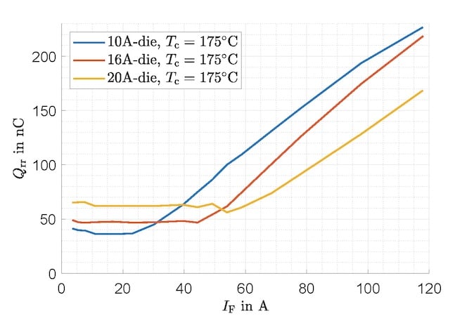
Figure 1. Reverse recovery charge Qrr at TC = 175°C for different die sizes. Image used courtesy of Bodo’s Power Systems [PDF]
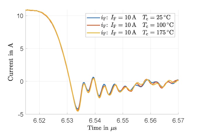
Further insight into the reverse recovery behavior is provided in Figure 2, which presents the measured current waveforms during diode turn-off. In Figure 2a, using IF = 10 A, the reverse recovery current shape remains nearly unchanged across the entire temperature range, confirming the absence of significant bipolar injection below the threshold. In contrast, Figure 2b highlights the behavior at 175 °C as the forward current increases.
At IF = 60 A, a pronounced increase in reverse recovery charge is observed, consistent with the onset of charge carrier injection beyond the critical threshold. Importantly, even in this regime, the behavior does not indicate thermal runaway. The results underline that bipolar effects remain controlled and only become significant beyond specific operating points, supporting the robustness of the investigated SiCMPS diodes under extreme conditions.
(a)
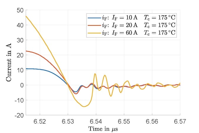
Figure 2. Reverse recovery current waveforms (a) at IF = 10 A for different temperatures (b) at TC = 175°C for varying IF. Image used courtesy of Bodo’s Power Systems [PDF]
The devices were subjected to extreme stress conditions, including reverse currents up to 20 times the nominal rating, case temperatures of 175 °C and current slopes of up to 9 A/ns. Despite these conditions, none of the tested diodes showed any signs of electrical or thermal failure.
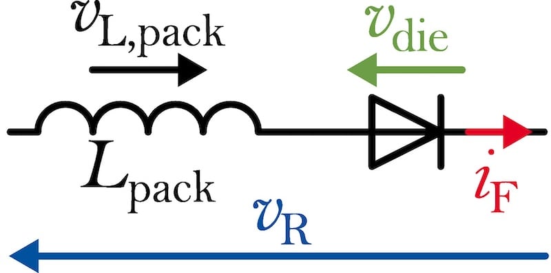
Figure 3. Diode parameter definition. Image used courtesy of Bodo’s Power Systems [PDF]
Using the definitions in Figure 3, the internal die voltage vdie(t) can be reconstructed over time. This is based on the measured package voltage vR(t), the known package inductance, and the current through the diode, as described in equation (3) [4].
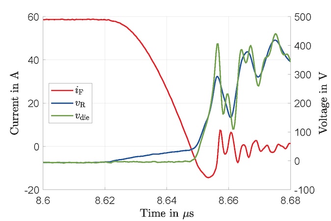
Figure 4. Waveforms of vR(t), vdie(t), and iF(t) during reverse recovery. Image used courtesy of Bodo’s Power Systems [PDF]
\[v_{die}(t)=v_{R}(t)+L_{pack}\cdot\frac{di_{F}(t)}{dt}\,\,\,\,\,\,\,\,\,\,(3)\]
Figure 4 illustrates the waveforms of the measured voltage vR(t), the reconstructed die voltage vdie(t), and the diode current iF(t). A significant voltage overshoot at the die level was observed during steep current transitions. This overshoot is influenced not only by the di/dt but also by the corresponding package inductance.
Package inductance parasitics have an impact on the voltage stress at the chip level. Higher inductance causes increased voltage overshoot during commutation events. Transient voltages, derived as described in equation (3), reached up to 900 V on devices rated for 650 V. Nevertheless, no destructive overvoltage conditions were observed.
Discussion: Implications for Application Engineers
The experimental results highlight the robustness of Nexperia’s SiC-MPS diodes under demanding electrical and thermal stress. Although the reverse recovery behavior changes beyond certain current and temperature thresholds, it remains nearly constant across a broad operating range. None of the tested devices experienced electrical or thermal failure, even under extreme conditions, underscoring their resilience.
This suggests that the diodes can tolerate short-term dynamic overloads without functional interruption. Such conditions may arise temporarily, for example, during cold-start events or transient overcurrent peaks. While these findings do not replace formal specification limits, they offer valuable insight into safe operating behavior under real-world conditions.
For system design, this reveals potential benefits in pulsed or fault-tolerant applications. The ability to withstand brief overstress events with stable switching behavior may provide additional design margin and support more compact, cost-efficient solutions. However, package parasitics, especially their impact on voltage overshoot, have to be carefully considered. Appropriate gate resistor selection and optimized PCB layout are essential to limit transient voltage spikes and ensure reliable operation.
The observed performance under combined high current and temperature conditions supports the applicability of these diodes in safety-critical systems such as automotive on-board chargers. In operating regimes where bipolar carrier injections occur, the devices continued to switch reliably. Although changes in reverse recovery characteristics were observed, the bipolar effects themselves appear to contribute to stable thermal behavior under elevated stress.
Ultimately, application-specific validation remains essential. While the results indicate a certain degree of design headroom, system-level testing is necessary to address the dynamic conditions of real-world use. These insights may contribute to a more differentiated approach to derating and component selection, helping to optimize cost, size, and thermal performance in practical designs.
Conclusion
These investigations demonstrate that SiC-MPS diodes from Nexperia exhibit robust switching behavior under demanding electrical and thermal stress. In all tested scenarios, the devices withstood elevated transient conditions, confirming their suitability for use in environments with high reliability demands. These findings may support greater design flexibility, particularly in applications in which short-term current peaks have to be managed safely.
The results highlight the diodes’ potential for safety-critical systems such as automotive on-board chargers. Further work could address system-level validation and compare measured device behavior with simulation results of corresponding models to support robust design under dynamic stress.
References
[1] Nexperia, Diode Application Handbook: Fundamentals, Characteristics, Applications. 2022.
[2] Nexperia, “PSC1065J 650 V, 10 A SiC Schottky Diode in D2PAK R2P: Product Data Sheet,” 2024.
[3] J. Lutz, H. Schlangenotto, U. Scheuermann, and R. W. de Doncker, Semiconductor Power Devices: Physics, Characteristics, Reliability (Electrical Engineering), Second edition. Cham: Springer, 2018.
[4] S. Ginzel, K. Hoffmann, Z. Yu, S. Fahlbusch, and S. Habenicht, “SiC MPS Diodes – Impacts of Package Inductance and Charge Carriers on Dynamic Switching Behavior” in Proceedings of PCIM Europe 2025; International Exhibition and Conference for Power Electronics, Intelligent Motion, Renewable Energy and Energy Management, 2025, pp. 1–7.
This article originally appeared in Bodo’s Power Systems [PDF] magazine and is co-authored by Simon Ginzel, Professorship of Power Electronics, Helmut-Schmidt-University, Hamburg/Germany; Zhe Yu, Principal Power Application Engineer, and Bengt Sprätz, Product Application Engineer, both Nexperia, Hamburg/Germany.