Facebook
 Google
 GitHub
 Linkedin
1200V CoolSiC™ MOSFET: High Performance Complemented by High Reliability
This article discusses the advantages and benefits of applying Infineon's SiC MOSFETs with blocking voltages of 1200V in various application fields.
Silicon Carbide (SiC) switches become increasingly more important for differentiation of power converters in size, weight and/or efficiency. The dedicated material properties of SiC enable the design of minority carrier-free unipolar devices instead of the charge modulated IGBT devices. As such, they deliver the highest efficiency, higher switching frequencies, reduced heat dissipation and space savings – benefits that, in turn, also lead to overall lower cost.
In addition to the static and dynamic performance, further topics need to be addressed to be ready for higher volume inverter use. Proper reliability is mandatory as well as sufficient threshold voltage and applications-oriented short-circuit robustness. IGBT compatible driving with VGS= 15 V for turn-on will simplify the change from IGBT to SiC MOSFET solutions. These topics are addressed with the new 1200V CoolSiC™ MOSFET from Infineon.
Introduction
SiC MOSFETs with blocking voltages of 1200V are interesting in application fields such as solar converters, UPS, battery chargers as well as industrial drives. These applications benefit from the reduction of switching and conduction losses; the thermal budget can be utilized to achieve higher switching frequencies to reduce the physical size of passive components and minimize the cooling effort, weight and cost.
The CoolSiC™ complemented by T- MOSFET design was developed to limit the electric field in the gate oxide in on-state as well as in off-state. An attractive specific on-resistance for the 1200V class is provided, achievable even in mass production in a stable and reproducible way. The low on-resistance is already achieved at driving voltage levels of only VGS= 15 V combined with a gate-source-threshold voltage of more than 4V being a benchmark in the landscape of SiC transistors. These boundary conditions are the baseline for transferring quality assurance methodologies established in the silicon power semiconductor world in order to guarantee FIT rates expected in industrial and even automotive applications.
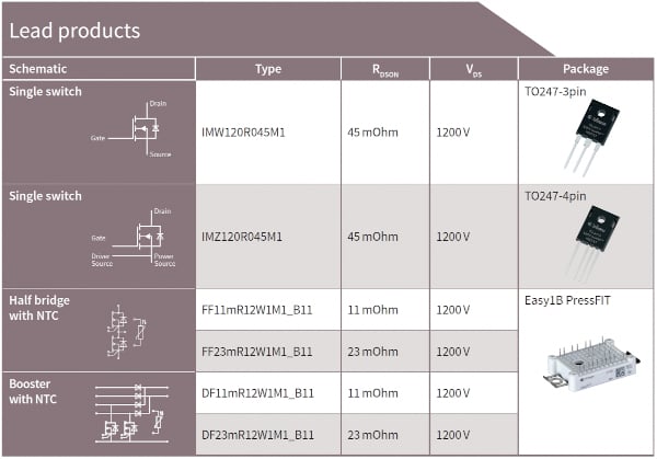
Figure 1: CoolSiC™ MOSFET lead product overview
For fast switching IGBTs and SiC transistors, the design of the package is equally important.
With a look to the available power module platforms, some packages are extremely advantageous towards fast switching SiC devices. The stray inductances need to be as low as possible, but in addition, a highly symmetric design is needed as well.
The Easy-Module platform, for example, is predestined for this use. In contrast to well-known standard packages with baseplate, the Easy-Module platform allows building a highly symmetric, low inductive design. For this reason, the popular and flexible Easy1B power module is used to implement a first SiC half-bridge and booster solutions optimized for photovoltaic, off-board electric vehicle charging and uninterruptable power supplies.
The flexible pin grid of Easy modules simplifies PCB layout and offers a stray inductance below 10nH. This is a huge improvement, a step down by 70-80% compared to existing solutions like EconoDUAL™, or standard SIXPACK designs. It represents a significant innovation in power module design.
Figure 1 depicts an overview about the lead products. The listed products are just the first step getting the broadly optimized portfolio of CoolSiC™ MOSFET products with further devices currently under development.
Device design philosophy
Switching losses of SiC-MOSFETs are usually quite low and especially almost temperature independent. Advanced design activities focus on the area specific on-resistance as the major benchmark parameter for a given technology. For 4H-SiC based planar MOSFETs an extraordinary high interface trap density close to the conduction band has to be overcome. This ends up at very low channel mobilities and therefore high contributions of the channel to the total on-resistance. The high defect density is reflected in various peculiarities of SiC-MOSFET based devices. An observed way to overcome this dilemma is to increase the electric field applied across the oxide in on-state, exceeding values usually being used in silicon-based MOSFET-devices. Such high fields in the oxide in the on-state can potentially accelerate the wear out. This can be seen as a long term reliability risk, in particular with respect to the high defect density of SiC-substrates.
Based on those considerations, it is obvious that planar MOSFET-devices in SiC have actually two sensitive areas with respect to oxide field stress, as sketched in the left part of figure 2

Figure 2: Left part: Typical structure of a planar MOSFET revealing two sensitive areas with respect to oxide field stress. Right part: Typical structure of a Trench-MOSFET, critical issue is the oxide field stress at the trench’s corners.
First, the usually discussed stress in reverse mode in the area of highest electric field close to the interface between the drift region and gate oxide and second the overlap between gate and source which is stressed in on-state.
A high electric field in on-state is seen as more dangerous since no device design measures are in place which could reduce the field stress during on-state. Thus, the overall goal is to combine the low RDSon potentially offered by SiC with an operation mode where the part remains in the well-investigated safe oxide field-strength conditions. In the on-state, this can be achieved today by moving away from the planar surface with its high defect density towards other, more favorable surface orientations.
Gate Oxide Reliability
The challenge regarding the gate oxide reliability of SiC MOS devices is to ensure a low enough failure rate, including extrinsic defects, throughout a desired lifetime under given operation conditions. The typical industrial requirement targets of << 100 ppm in 20 years of operation. The root cause for extrinsic defects in the gate oxide of SiC MOS devices is mainly ruled by defects within the substrate material, epitaxial process and, to a less significant contribution, by the remaining process chain. Tests of commercial MOSFET products reveal that this issue is still a serious concern for the use in industrial systems.
Therefore, long time tests with a larger number of devices were performed to investigate extrinsic gate oxide failure rates for Infineon’s CoolSiC™ MOSFET. An experiment was done in two groups of 1000 discrete devices each, performed at 150°C under constant gate bias stress for three sequences of100 days. Figure 3 summarizes the test results. After 100 days, the gate-source voltage was increased by +5 V.
These statistics fit well to the linear E-Model. An acceleration factor was determined for best fit corresponding to the solid lines in figure 3.
By extrapolating this result to an operation lifetime of the device of 20 years using the recommended voltage levels, the model predicts a failure rate of 0.2 ppm. Hence, there is evidence to have a reliability of the gate oxide similar to the one known from IGBTs, which fits perfectly to the typical industrial requirement.
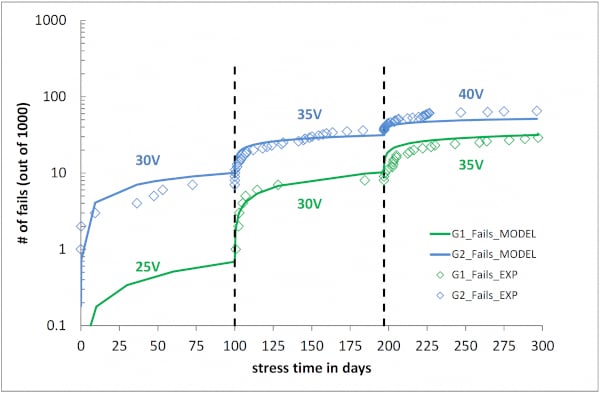
Figure 3: Long term test: the number of fails is plotted over stress days. In total 2 groups of 1000 devices were tested at 150°C with constant gate voltage VGS which is indicated. VGS is increased by 5 V every 100 days. Each dot represents a fail. Solid lines represent the prediction by linear E model
Dynamic Performance
Being a unipolar device, the dynamic performance of the SiC-MOSFET is mainly ruled by its capacitances. The device was designed to have a small Gate-Drain reverse capacity Crss compared to the input capacity Ciss. This is beneficial to prevent the MOSFET from parasitic turn-on and sophisticated gate driver circuitry when operated in a half-bridge configuration.
Figure 4 displays the typical switching losses of a half-bridge with single devices mounted in a 4-pin TO-247 housing as a function of drain current. The turn-off energy Eoff is nearly independent of the load current since it is dominated by capacities, whereas the turn-on energy Eon increases linearly with current.
At an application current of 20 A, the total losses Etot sum up to 0.43 mJ which enables switching frequencies in the range of 50-150 kHz.
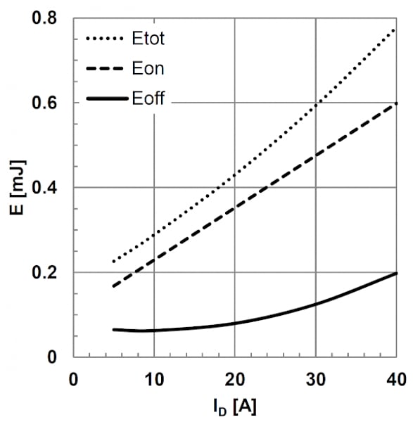
Figure 4: Typical switching energies as a function of drain current ID.
Conditions: VGS = 15 / -5 V, RGext = 4.5 Ω, VDS = 800 V, Tvj =175° C, 4 leg TO-247 in half-bridge configuration
The 4th pin of the TO-247 package is to connect the gate driver directly to the source pin, avoiding the negative feedback from the load current due to source stray inductances. Thus, in comparison to a 3-leg TO247 half-bridge configuration, about 100 µJ total switching energy can be saved at a current of 20 A. This is a reduction of about 30% based only on the optimization of the package using the same die.
Figure 5 provides an insight to the MOSFET’s ability to easily control the voltage slope dv/dt by adapting the gate resistor RG. This is particularly of interest for drives applications. However, the reduced voltage slope dv/dt is paid for by increased switching losses.
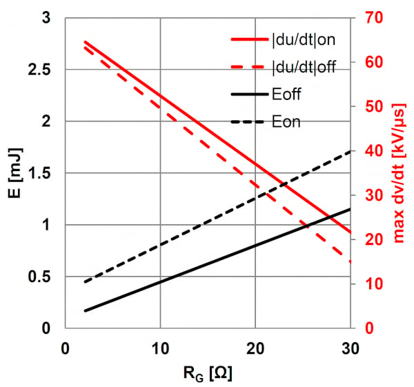
Figure 5: Typical switching losses (left axis, black curves) and
maximum dv/dt values (right axis, red curves) vs. RGext.
Conditions: VDS=800 V, ID = 40A, VGS = 15 / -5 V, Tvj=175°C, 3 leg TO-247 in half bridge configuration
Obviously, the loss reduction will be more prominent in applications where there is no dv/dt limitation and grows with the switching frequency. This is common in DC-DC boost or buck/boost topologies, providing the benefit of smaller, lighter and lower cost magnetic components. Various studies have already proven that – even with more expensive power switches – the cost of material can be reduced for a wide spectrum of applications. This number of applications will increase over the mid-term time frame based on the anticipated cost reduction over time for SiC-based components.
Static Performance
The key parameter of the static output characteristic of a MOSFET is the total resistance RDS(ON). The newly introduced die features a typical on-resistance of 45 mΩ at room temperature at VGS = 15 V. A positive temperature coefficient of the on-resistance makes the devices predestined to be used for paralleling. In Figure 6 the output characteristic is given in direct comparison to the state of the art 1200 V HighSpeed 3 IGBT. Due to the knee voltage on state characteristic the conduction losses especially under partial load can be reduced enormously. At system level, the feature of knee voltage free conduction behavior offers a significant potential for loss reduction. Many systems are operated under partial load conditions for a large portion of their life and conduction losses are considerably lower compared to the competing standard IGBT technologies. Even at very low switching frequencies of less than 5 kHz and unchanged dv/dt slopes, it can be seen that a knee voltage-free switch with integrated body diode, in synchronous rectification mode, offers a potential of 50 % total loss reduction compared to a commercial IGBT solution available today.
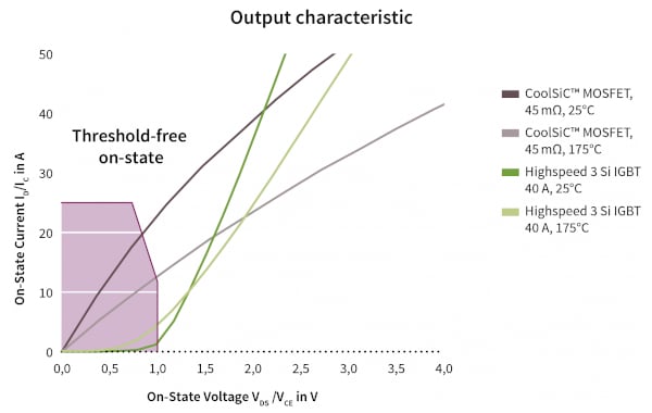
Figure 6: Typical SiC-MOSFET output characteristic in comparison to IGBT solutions
In contrast to booster-stages, typical inverter applications require a well-defined short circuit capability especially in case of failure events in the field. Reflecting this important need, the CoolSiC™ MOSFET is the first SiC-MOSFET on the market with a specification of short circuit robustness.
In contrast to typical DMOS behavior the transfer characteristics (25°C /175°C) reveal a crossing point already at VGS = 12 V. Above 12 V, the current decreases with temperature which is beneficial to limit the saturation current in a short circuit event.
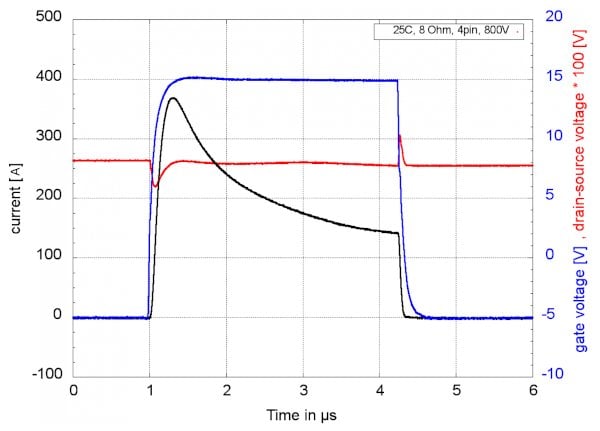
Figure 7: Typical short circuit behavior of CoolSiC™ MOSFET in TO-247-4
Figure 7 denotes the most critical, so-called hard short circuit event. The behavior and robustness under this special condition was analyzed in detail. The CoolSiC™ MOSFET is the first SiC MOSFET with short circuit specification.
In contrast to standard IGBTs, the short circuit current rises to a factor of 10 compared to the nominal current of the device. After the first peak the saturation current decline to a much lower level due to the temperature depending characteristics described above.
Summary
Infineon is a pioneer in the commercial use of the SiC technology. As the first company worldwide, SiC-based diodes were introduced in the market as early as 2001. Meanwhile, the 5th generation of such parts is available as discrete devices. The product design was always carefully oriented on a beneficial cost-performance evaluation.
The concept of Infineon’s SiC-Trench-MOSFET combines a low on-resistance with an optimized design preventing too high gate oxide field stress, providing IGBT like gate oxide reliability. The SiC-Trench-MOSFET features superior performance in terms of switching behavior and losses. The analysis done confirms a full controllability of the voltage slopes in booth, turn-on and turn-off transients. The current slopes for turn-on as well can be controlled by the gate resistor. In turn-off, the di/dt is determined by parasitic capacitive effects.
Furthermore, the device is the best available mix of electrical performance and robustness features like the short circuit reliability.
With the CoolSiC™ MOSFET technology, the beginning of a new era of power electronics in terms of power conversion efficiency and power density has begun.
About the Author
Marc Buschkühle works as the Head of the Technical Marketing High Power Modules at Infineon Technologies AG, Warstein, where he is responsible for the Technical Marketing team and products for High Power Modules covering high voltage (Voltages greater than or equal to 1.2 kV) and high power (greater than 200 kW) application within Infineon.
This article originally appeared in the Bodo’s Power Systems magazine.