Facebook
 Google
 GitHub
 Linkedin
The Next Generation of SiC Power Modules
This article features Mitsubishi Electric SiC power modules as next big step in modern power electronics for high-power converters with high current ratings.
Since years, Mitsubishi Electric is well-known for its high-current SiC Power Modules, available in different voltage classes. For 1200 V and 1700 V, the second generation SiC Power Modules is released now. Compared to the first generation, the performance has been improved and a wider line-up will be available. As one promising technology for 3300 V and 6500 V SiC Power Modules, Mitsubishi Electric is embedding the Schottky diode into the MOSFET chip. For this cutting-edge technology, latest research results are presented.
Introduction
The use of silicon carbide (SiC) is the one big evolutionary step in modern power electronics. Due to the physical properties, power electronics made of SiC are more powerful and more efficient compared to classical silicon materials. Mitsubishi Electric has started the development of SiC power semiconductors already in the early 1990s.
SiC devices for various voltage and current ratings
Over the past decade, Mitsubishi commercialized many SiC devices for various voltage and current ratings putting special focus on large SiC-chips and high current SiC-modules. In several applications, such as elevators, uninterruptable power supplies, photovoltaics or railway, the use of Mitsubishi high power SiC-modules allows outstanding system performances and power densities.
This article presents the latest information of Mitsubishi’s research and development in the field of SiC Power Modules. For the 1200 V and 1700 V class, the 2nd generation is introduced. The technical innovations as well as the performance increase compared to the previous generation is discussed.
Challenges of SiC-MOSFETs
For higher voltage ratings, one of today’s challenges of SiC-MOSFETs is the degradation of the body diode. An answer to this problem is the use of a Schottky Barrier Diode (SBD) anti-parallel to the SiC MOSFET. The Mitsubishi specific approach is integrating the SBD into the MOSFET chip. This approach allows significant increase in power density of high-voltage SiC devices. The details are explained for a 3300 V and 6500 V device in the final chapter.
Second Generation 6-inch SiC Modules
In the following, Mitsubishi’s 2nd generation of 4H-SiC MOSFETs rated for 1200 V and 1700 V are introduced (see [1] for information on 600 V SiC MOSFETs). The 2nd generation 1200 V SiC MOSFETs, as shown in Figure 1, manufactured on the newly developed 6-inch SiC wafer line, feature an optimized p-well, a cell-pitch shrinkage and an optimized channel-doping profile as illustrated in Figure 2 [2]. This results in an improved gate-oxide reliability and a reduction of the conduction loss.
Specific resistance Ron sp at room temperature of 1st and 2nd generation
Figure 4 shows the specific resistance Ron, sp at room temperature of 1st and 2nd generation 1200 V MOSFET chips rated for 100 A/cm². Consequently, the resistance decreases by 33% from 4.5 mΩ∙cm² to 3.0 mΩ∙cm² by the optimized cell structure. When the cell pitch is decreased, the JFET region becomes narrower as well. If the JFET width becomes too narrow, it will become a bottleneck and the ON-state resistance will increase. By special doping of the JFET region, however, Mitsubishi solved this problem.
How the ON-state resistance is reduced
Figure 3 shows how the ON-state resistance is reduced by an optimized JFET doping. With the optimized JFET doping, these cutting-edge planar MOSFETs are able to compete against today’s trench structures as illustrated in Figure 6. At the same time, the planar structure has lower complexity compared to a trench gate structure.
The switching performance of the 2nd generation has been improved as well. The reverse transfer capacitance (or Miller capacitance) has become smaller. This allows faster switching speeds. As shown in Figure 5, turn-ON and turn-OFF losses reduce by 23% and 37% respectively compared to the previous generation.

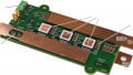
Figure 1: 2nd generation 1,200V Full-SiC module with RTC short-circuit protection

Figure 2: Cross section of a 1st and 2nd generation SiC MOSFET chip
Also for the 1700 V SiC MOSFETs, cell-pitch shrinkage and the optimized doping profile is applied. Reference [3] demonstrates the performance of these large-current chips packaged in a 300 A half-bridge module. Correspondingly, a VDS(on) of 2.75 V at 300A drain current and 150 °C junction temperature is achieved. The turn-ON and turn-OFF energies at 300 A and 150 °C are 12.0 mJ and 3.0 mJ respectively (at Rg = 1.6 mΩ ). These conduction and switching performances are among the best ever reported.

Figure 3: Impact of JFET doping on the ON-state resistance
Fast short-protection of SiC modules
Usually, we have to trade the lower RDS(on)off against short-circuit capability. Moreover, short-circuit protection is challenging for SiC in general. Therefore, Mitsubishi Electric has developed, already for the 1st SiC generation, the Real-Time Control (RTC) [4]. It allows inherent and fast short-protection of SiC modules.
Figure 7 and Figure 8 show the principle schematic of the RTC and the waveforms during a short circuit respectively. If the RTC detects a short circuit, it will automatically reduce the gate voltage to limit the short-circuit current magnitude.
Therefore, the energy dissipated in the SiC-MOSFET during SC-mode is reduced. This means the user can design his gate driver and his gate conditions without requiring too fast SC-precautions.
The RTC gives effective protection against short circuit and has been well accepted already for 1st gen SiC modules. Consequently, Mitsubishi Electric will provide the RTC feature for the complete lineup of the 2nd generation from 300 A to 1200 A as summarized in Table 1.
![Figure 4: Typical output characteristic of 1st and 2nd generation 1200 V SiC MOSFETs [2]](https://eepower.com/uploads/thumbnails/1877-4179-mitsubishi-electric-europe-bv-mitsubishi-electric-europe-bv-mitsubishi-electric.jpg)
Figure 4: Typical output characteristic of 1st and 2nd generation 1200 V SiC MOSFETs [2]
![Figure 5: Switching waveforms of 1st and 2nd generation 1200 V SiC MOSFETs (left: turn-ON, right: turn-OFF) [2]](https://eepower.com/uploads/thumbnails/1877-4180-mitsubishi-electric-europe-bv-mitsubishi-electric-europe-bv-mitsubishi-electric.png)
Figure 5: Switching waveforms of 1st and 2nd generation 1200 V SiC MOSFETs (left: turn-ON, right: turn-OFF) [2]
SiC Modules for High-Voltage Applications
A well-known and widely discussed degradation mechanism in SiC semiconductor material is the so-called bipolar degradation (BPD) (cf. Figure 10). Today we know that a bipolar current through the internal body diode of the SiC-MOSFET may cause a dislocation of the SiC lattice. This dislocation can be the reason for an irreversible degradation mechanism [5] [6].
Mitsubishi’s strategy to prevent BPD is the connection of a SiC Schottky barrier diode (SBD) in parallel to the MOSFET’s body diode.

Figure 6: Resistance comparison of different planar and trench type 1200V SiC MOSFETs

Figure 7: Schematic of Real Time Control (RTC) for inherent short-circuit protection
| 1200V | 1700V | |||
| without RTC | with RTC | without RTC | with RTC | |
| 300 A | - | 4-in-1 | - | 2-in-1 |
| 400 A | 4-in-1 | 4-in-1 | - | - |
| 600 A | - | 2-in-1 | - | - |
| 800 A | 2-in-1 | 2-in-1 | - | - |
| 1200 A | - | 2-in-1 | - | - |
| *2-in-1: half-bridge module 4-in-1: full-bridge module |
||||
Table 1: Planned line up 2nd generation SiC
When the voltage drop of the SBD is small enough, the SBD will take over the current and will prevent bipolar current flow through the body diode. In 4 years of field-experience with a 3300 V Full-SiC device, the ruggedness against BPD has been proven using this method.
SBD chip area
The SBD chip area is used to prevent bipolar current dependents on the device voltage. For a 3300 V device, the SBD chip area in relation to the MOSFET are is 1.3-times. For a 6500 V device, however, it is already 3-times. Since this would lead to a poor utilization of chip mounting area in the power modules, Mitsubishi investigates more advanced strategies for high-voltage devices.
Embedding the SBD
Embedding the SBD into the MOSFET chip is a promising approach, which has been demonstrated for a 6500 V SiC-MOSFET already [7] [8]. As illustrated in Figure 11, the new SBD-embedded MOSFET structure results in smaller total chip area, thus allowing enhanced density of the power module.

Figure 8: RTC operation during short circuit


Figure 9: 3.3 kV and 6.5 kV Full-SiC modules for high-voltage applications in the LV100 (left) and HV100 (right) package

Figure 10: Illustration and picture of bipolar degradation (BPD) due to stacking faults
Furthermore, embedding the SBD, leads to superior switching characteristics as demonstrated in [9] for a 3300 V device. Figure 12 shows the switching waveforms for the SBD-embedded MOSFET (A – blue), MOSFET with external SBD diodes (B4 – green) and, for comparison, solely the MOSFET without diode (C – red).
Consequently, the SBD-embedded MOSFET has the lowest switching losses, because the total charge Qtot is the smallest of all devices.
As a result, the losses during MOSFET turn-ON are reduced by 20% compared to the external SBD diode. Moreover, compared to the MOSFET without SBD, the SBD-embedded device is free from bipolar degradation and has superior power density.

Figure 11: Comparison between conventional MOSFET and SBD-embedded MOSFET
![Figure 12: Chip layout and diode turn-OFF waveform of the SBD-embedded (A), external SBD diode (B4) and without SBD diode (C) [9]](https://eepower.com/uploads/thumbnails/1877-4188-mitsubishi-electric-europe-bv-mitsubishi-electric-europe-bv-mitsubishi-electric.jpg)
![Figure 12: Chip layout and diode turn-OFF waveform of the SBD-embedded (A), external SBD diode (B4) and without SBD diode (C) [9]](https://eepower.com/uploads/thumbnails/1877-4187-mitsubishi-electric-europe-bv-mitsubishi-electric-europe-bv-mitsubishi-electric.png)
Figure 12: Chip layout and diode turn-OFF waveform of the SBD-embedded (A), external SBD diode (B4) and without SBD diode (C) [9]
Conclusion
Converters utilizing SiC power modules are the next big step in modern power electronics. They enable best-in-class power densities and highest efficiencies. In all voltage classes, Mitsubishi Electric offers SiC Power Modules with high current ratings, which are required for high-power converters. Now, Mitsubishi launches the second generation of 1200 V and 1700 V SiC Modules. The performance of these devices has been increased further and, utilizing the RTC technology, they are protected against short-circuits.
For 3300 V and 6500 V, the development of MOSFET chips with integrated SBD diode enables Power Modules with high power densities. After starting the development of SiC devices in the 1990s, Mitsubishi Electric today offers a large SiC line-up from 1200V to 3300V. Module with even higher voltages are under development.
Acknowledgement
This work is partially supported by New Energy Industrial Technology Development Organization (NEDO).
About the Authors
Dr. Nils Soltau is working at Mitsubishi Electric Europe B.V within the semiconductor department, in which Mitsubishi Electric is one of the world's leading names in the manufacture and sales of electrical and electronic products and systems used in a broad range of fields and applications.
Dr. Eckhard Thal is graduated with diploma in electrical engineering at the Moscow Institute for Energy in. 1980. He received his PhD 1991 in.
Toru Matsuoka is an inventor working at Mitsubishi Electric Corporation, Fukuoka, Japan. He has filed filed for patents to protect the following inventions and has listed several patents applications that are pending, as well as patents that have already been granted by the United States Patent and Trademark Office (USPTO).
References
- Y. Ebiike, T. Tanioka, M. Furuhashi, A. Osawa and M. Imaizumi, “Char-acteristics of High-Threshold-Voltage Low-Loss 4H-SiC MOSFETs with Improved MOS Cell Structure,” Materials Science Forum, no. 858, pp. 829-832, 2016.
- T. Tanioka, Y. Ebiike, Y. Oritsuki, M. Imaizumi and M. Tarutani, “High Performance 4H-SiC MOSFETs with Optimum Design of Active Cell and Re-Oxidation,” in PCIM Europe, Nuremberg, Germany, 2018.
- K. Hamano, Y. Oritsuki, T. Tanioka, N. Hanano, M. Imaizumi, E. Sueka-wa, M. Tarutani and Y. Miyazaki, “2nd generation High performance 4H-SiC MOSFETs with 1.7 kV rating for high power applications,” in PCIM Europe, Nuremberg, Germany, 2019.
- E. Thal, K. Masuda and E. Wiesner, “New 800A/1200V Full SiC Mod-ule,” Bodo’s Power Systems, pp. 28-31, Apr 2015.
- H. Jacobsson al. et., “Properties of Different Stacking Faults that Cause Degradation in SiC PiN Diodes,” in Materials Science Forum, Switzerland, 2003.
- P. O. A. Persson et. al., “Structural defects in electrically degraded 4H-SiC p+/n-/n+ diodes,” Applied Physics Letters, vol. 80, no. 25, pp. 4852-4854, 24 06 2002.
- S. Hino, H. Hatta, K. Sadamatsu, Y. Nagahisa, S. Yamamoto, T. Iwamatsu, Y. Yamamoto, M. Imaizumi, S. Nakata and S. Yamakawa, “Demonstration of SiC-MOSFET Embedding Schottky Barrier Diode for Inactivation of Parasitic Body Diode,” Material Science Forum , no. Vol. 897, pp. 477-482, 2017.
- K. Kawahara and S. Hino et. al., “6.5 kV Schottky-Barrier-Diode-Em-bedded SiC-MOSFET for Compact Full-Unipolar Module,” in 29th Int. Symposium on Power Semiconductor Devices & ICs, Sapporo, 2017.
- T. Tominaga, S. Hino, Y. Mitsui, J. Nakashima, K. Kawahara, S. Tomo-hisa and N. Miura, “Superior Switching Characteristics of SiC-MOSFET Embedding SBD,” in 31st International Symposium on Power Semi-conductor Devices & ICs, Shanghai, China, 2019.
- Mitsubishi Electric Corporation, Mitsubishi Electric’s New 6.5 kV Full-SiC Power Semiconductor Module Achieves World’s Highest Power Density, Japan: Press Release No. 3164, 2018.
- J. Yamada and E. Thal, “SiC Power Modules for a Wide Application range,” Bodo’s Power Systems, pp. 20-27, Sep. 2017.
- N. Soltau, E. Wiesner, R. Tsuda, K. Hatori and H. Uemura, “Impact of Gate Control on the Switching Performance of a 750A/3300V Dual SiC-Module,” in 20th European Conference on Power Electronics and Applications (EPE’18 ECCE Europe), Riga, 2018.
- N. Soltau, E. Wiesner, K. Hatori and H. Uemura, “3.3 kV Full SiC MOS-FETs - Towards High-Performance Traction Inverters,” Bodo’s Power Systems, no. 01, pp. 22-24, 2017.
- J. Yamada and E. Thal, “Gaining Speed: Mitsubishi Electric SiC-Power Modules,” Bodo’s Power Systems, pp. 22-30, Sep. 2018.
This article originally appeared in the Bodo’s Power Systems magazine.