Facebook
 Google
 GitHub
 Linkedin
SiC LinPak Designed for Improved Switching Performance, Reliability
Each day that we wake up and turn on a light, the coffee machine, or electric stove to prepare breakfast, we expect all the electric motors, heaters and light bulbs to work perfectly. Despite the billions of devices in operation worldwide – all of which are expected to work at the flip of a switch - every day we add even more systems that require 100% reliable delivery of electricity. So much so that electricity demand has doubled in the last two decades and is expected almost double yet again in the next two decades.
On one hand, electricity production must be increased to meet increased demand. This increase needs to come from sources that are not harmful to the environment, such as off- and on-shore wind, photovoltaics, pump-hydro generation, and other renewable power-generation technologies.
On the other hand, distributing the generated electricity where it is needed has to be done reliably and with as little loss as possible. In the chain that converts the energy source into electricity, heat, light or mechanical movement, the power semiconductors at the core of electronic systems are key to improving energy conversion efficiency.
To increase efficiency and reduce the overall environmental impact of energy systems, novel semiconductor materials must deliver higher power at lower losses. They also need packages that enable higher current densities by decreasing thermal resistance while simultaneously increasing expected lifetime.
The LinPak is a power semiconductor package that is establishing itself as standard in diverse applications including traction, wind converters, battery storage systems, photovoltaic, medium- and low-voltage drives, solid-state transformers, etc. In the quest to increase efficiency, new semiconductor materials such as SiC are used. SiC has a series of unquestionably better characteristics when compared to Si, particularly higher electric field strength and thermal conductivity. In this article, we provide a glimpse into the process of designing such a device and how to optimize it for better performance in customer applications.
SiC With High K Dielectric
The superior characteristics of SiC make a module with SiC MOSFETs much more compact, with only a fraction of the switching losses typically associated with a corresponding Si IGBT module. The biggest challenges with SiC are cost and reliability. For instance, the gate dielectric, especially the interface to the semiconductor, is highly sensitive to degradation.
On one hand, due to the higher permittivity and therefore higher dielectric capacitance (CD = εD/tD), the HKMOSFET has lower RDSon than a SiO2 gate dielectric (Figure 1). On the other hand, and even more important, it reduces the density of interface trap states (Dit), which results in unmatched robustness of the threshold voltage Vth, even after thousands of cycles of VGS sweep from +15 V to -15 V (Figure 2). This ensures that the switching characteristic will remain constant even if the device is subjected to un-wanted gate voltage swings during operation. Further device performance optimization is achieved by increasing the channel width and decreasing the device pitch. This will reduce the on-resistance RDSon as well as switching losses.
Module Design Optimization
The defect density for SiC dies is one of the main factors that increase the cost. To keep the dies affordable, they are manufactured in a small footprint (i.e., 5X5 mm). The challenge created by the small die size is that for a comparative rating -- as in the case of Si IGBT - a lot of SiC MOSFETs (up to 40 pcs) need to be connected in parallel within the LinPak module.
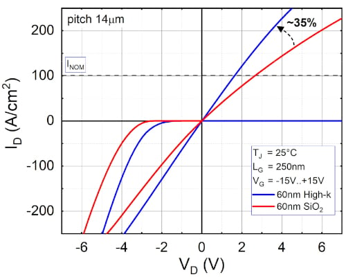
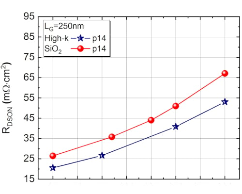
Figure 1. Output characteristics (A) and RDSON from 25°C to 200°C (B) of high–k and SiO2 3.3kV MOSFETs with LG=250nm and cell pitch of 14µm.
Images used courtesy of Bodo’s Power Systems

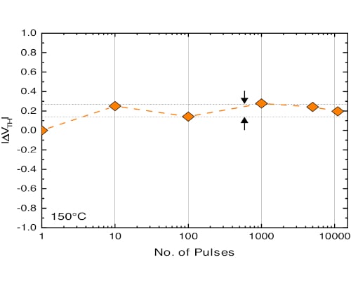
Figure 2. (A) Repetitive turn-on/off switching with extreme gate variation (B) variation of Vth during the repetitive VGS sweeps.
Images used courtesy of Bodo’s Power Systems
Such paralleling of fast switching SiC MOSFETs results in a significant electromagnetic design challenge. To provide low switching losses and reliable operation, fast switching without critical oscillations and balanced static and dynamic current sharing between MOSFETs must be ensured.
Since 2018, Hitachi Energy Semiconductors (formerly ABB) has introduced 1.7 and 3.3 kV SiC high-power modules developed on the LV LinPak platform. The SiC module exploited an innovative multilevel module concept that allowed for very flexible routing of the main current and the control signals. Based on this concept, fast and reliable switching has been demonstrated using up to 40 SiC MOSFETs connected in parallel within a single switch. Additionally, in combination with an optimized test setup, module switching losses close to the ones of the discrete devices can be achieved [7].
Hitachi Energy Semiconductors has collected user feedback for several years and used it to further improve the module design. A new, second generation of SiC LinPak has now been developed that focuses on:
- Improved module performance with even lower switching losses
- Decreased complexity compared with the first-generation design for improved manufacturability
First generation SiC LinPak internal gate resistors (placed on each module substrate) were used to avoid gate oscillations across all operating conditions. Although those gate resistors made module switching very robust, they restrict the minimum switching losses of the module. Therefore, to decrease module switching losses even further, the existing electromagnetic design was further improved. The design was first analyzed to identify root causes of oscillations. After analysis, remedies were proposed and implemented in new module designs. These module designs were further optimized to minimize the need for internal gate resistors for safe operation and reduce overall module complexity.
In the process of module design optimization, the following steps - combined with iteration loops - were used:
- Parasitic inductances were determined and optimized using Ansys Q3D Extractor (Figure 3). The main goals were to achieve balanced stray inductance, balanced gate inductance and balanced, negative gate coupling between all MOSFETs connected in parallel. Figure 4 illustrates the improvement in gate inductance achieved by design optimization.
- Extracted parasitics were used to assess switching performance of each module design using SIMetrix. To achieve fast switching without critical oscillations, as well as balanced static and dynamic current sharing between semiconductor devices in the real module, a double-pulse test of the SiC LinPak based on 20 and 40 MOSFET dies per switch was simulated. During the simulations, voltage, current and control signals were monitored for each MOSFET forming both the upper and lower switch of the half-bridge.
A recently developed SPICE model, with several adjustable parameters, also enabled us to study the impact of deviations (tolerances) of MOSFET’s parameters on the module switching performance.
Four newly developed and optimized module designs showing the best balance of stray inductance, gate inductance and gate coupling between MOSFETs and switching transients without critical oscillations were used to assemble and test 1.7 kV SiC LinPaks. The prototypes were based on the same SiC MOSFETs as used in the previous module generation. Switching transients and switching losses of the prototypes were determined in the double-pulse test using the test setup optimized for fast switching SiC LinPak.
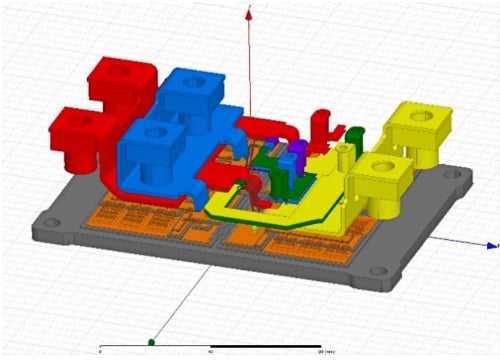
Figure 3. Q3D model of a complete SiC LinPak which was used to extract parasitics. Image used courtesy of Bodo’s Power Systems
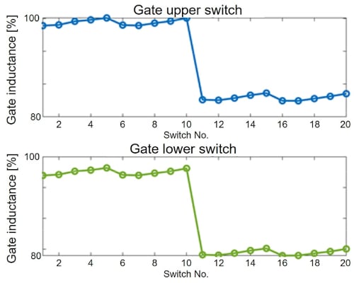
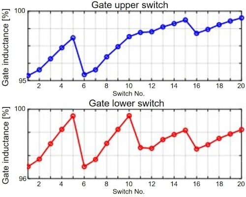
Figure 4. Improved balance of gate inductance achieved during the optimization process. (A) Gate inductance was determined for the previous version of SiC LinPak (upper and lower switch). Inductance is well balanced for switches 1-10 located on substrate 1 and switches 11-20 located on substrate 2. Max difference between devices located on one substrate is about 2%. However, the difference between MOSFETs located on different substrates, it is almost 20%. (B) Gate inductance was determined for the improved layout. Max difference between any two MOSFETs connected in parallel is less than 5% now. Images used courtesy of Bodo’s Power Systems
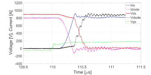
Concept 1 – Version 1. Turn-off (Rg_ext = 1.5 Ohm). Eon= 161.22 mJ. Image used courtesy of Bodo’s Power Systems
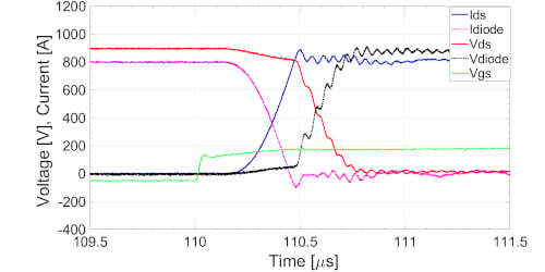
Concept 1 – Version 1. Turn-on (Rg_ext = 1.5 Ohm). Eon= 98.47 mJ. Image used courtesy of Bodo’s Power Systems
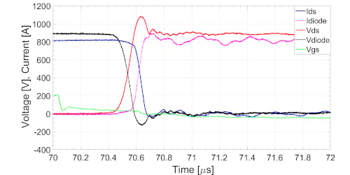
Concept 1 – Version 2. Turn-off (Rg_ext = 1.5 Ohm). Eon= 126.48 mJ. Image used courtesy of Bodo’s Power Systems
Concept 1 – Version 2. Turn-on (Rg_ext = 1.5 Ohm). Eon= 75.21 mJ. Image used courtesy of Bodo’s Power Systems
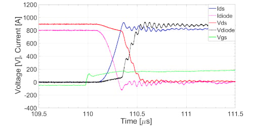
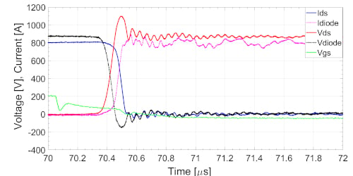
Concept 2 – Version 1. Turn-off (Rg_ext = 1.5 Ohm). Eon= 133.7 mJ Image used courtesy of Bodo’s Power Systems
Concept 2 – Version 1. Turn-on (Rg_ext = 1.5 Ohm). Eon= 80.56 mJ. Image used courtesy of Bodo’s Power Systems
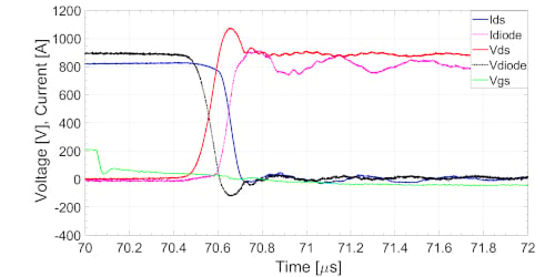
Concept 2 – Version 2. Turn-off (Rg_ext = 1.5 Ohm). Eon= 98.77 mJ. Image used courtesy of Bodo’s Power Systems
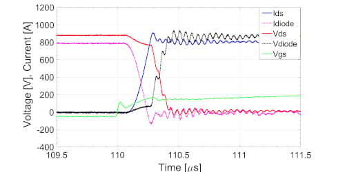
Concept 2 – Version 2. Turn-on (Rg_ext = 1.5 Ohm). Eon= 57.18 mJ. Image used courtesy of Bodo’s Power Systems
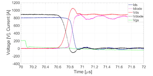
Figure 5. Switching transients measured for all four assessed module designs.
Figure 5 shows examples of turn-on and turn-off switching transients measured for all four tested module designs using an external gate resistor of 1.5 Ohm. The figure also includes corresponding switching losses.
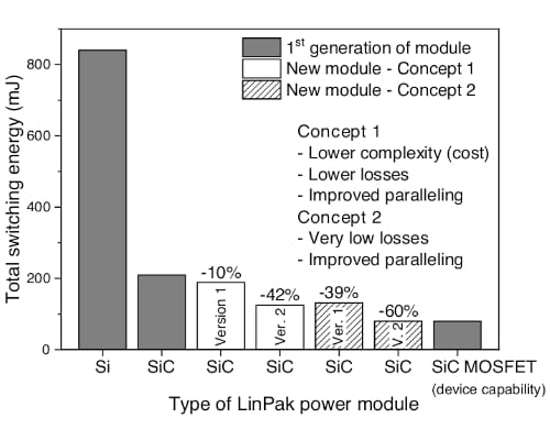
Figure 6. Comparison of total switching losses determined at 150 °C using an external gate resistor of 0 Ω (UDS = 900 V, ID=840A). From left to right: - Losses of Si IGBT module - First generation of SiC LinPak - Assessed concept 1 (version 1) - Assessed concept 1 (version 2) - Assessed concept 2 (version 1) - Assessed concept 2 (version 2) Numbers above bars indicate decrease of switching losses compared to the previous version of SiC LinPak. Image used courtesy of Bodo’s Power Systems
Figure 6 compares switching losses measured at 150°C if no external gate resistor was used. In all four cases, due to improved electromagnetic module design, lower or no internal (substrate) gate resistors were required and therefore switching losses were lower compared to first-generation SiC LinPaks. In one case, switching losses were even comparable to switching losses of a scaled discrete SiC MOSFET.
Output Simulations
To assess performance improvements in the new design of the SiC LinPak, a series of simulations were performed for a possible wind application. Two modules (20 MOSFET dies/ switch 5SFG 0900X170100, 40 MOSFET dies/switch 5SFG 1800X170100) were compared to the existing Si IGBT LinPak (5SNG 1000X170300).
| Simulation conditions | |
| Topology | 2 Level VSI |
| Fundamental frequency f | 10 Hz |
| Switching frequency fc | 2000 Hz |
| Control | Third harmonic injection |
| Phase current | I Ph f(fc) @ TvjMax or 600A |
| Power factor PF | 1.0 |
| DC Voltage | 1180 V |
| Voltage LL | 690 V RMS |
| Ambient temperature | 45°C |
| Rth Cooler | 11 K/kW |
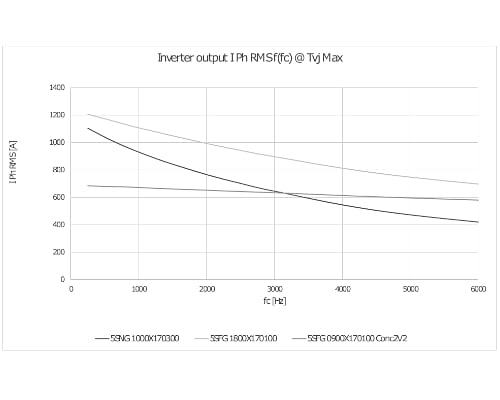
Figure 7. Current output vs. frequency for a 2 Level VSI. Image used courtesy of Bodo’s Power Systems
The much lower switching losses of the 900 A SiC module are apparent in the flat curve of current out vs. frequency (see figure 7). One also sees that when many MOSFET chips are packed in parallel, i.e., 40 pcs/switch, the switching speed needs to be slowed down, impacting switching losses. Even in this case, the 1800 A SiC module has a flatter current vs. frequency output. This means that for a given output current, i.e., 800 A, one can switch the LinPak module based on SiC MOSFETs twice as fast as the Si IGBT equivalent. This has obvious benefits for the filtering required.
In wind applications a very low fundamental frequency in the range of 10Hz is a big challenge because it causes, depending on the current load, a constant IGBT junction temperature ripple of 20-40 K. Calculated using an extreme case of continuous operation, more than 10 billion such cycles can be expected in the lifetime of the converter. When using the body diode for third quadrat operation, SiC MOSFETs use the same semiconductor area for both current directions, reducing the temperature ripple compared with an equivalent IGBT/ Free Wheeling Diode solution. This has substantial implications for the reliability of such modules.
Hitachi Energy Semiconductors has offered SiC LinPak demonstrator modules since 2018. In recent years, further work has been done to improve SiC MOSFET performance and robustness, as well as the LinPak package, to best suit these new, improved chips. The high-k dielectric on the MOSFET gate improves the key metric RDSon and dramatically increases its robustness when the gate is exposed to voltage swings.
The package was further optimized by performing electromagnetic simulations and electric tests to achieve the optimum compromise between switching losses, manufacturability and reliability. Finally, the performance of the module was simulated for the case of a two-level converter for wind application and compared with the standard IGBT/FWD module. SiC LinPak has proven to be the right choice for further improvements in the performance and reliability of a wide range of 21st century applications like wind, solar, traction, solid-state transformers and many others.
This article originally appeared in Bodo’s Power Systems magazine.