Facebook
 Google
 GitHub
 Linkedin
Effect of Optocoupler Parameter Variations on the Control Loop of a Power Supply
Isolated power supplies with secondary-side regulation need a feedback path to the primary side across the galvanic isolation. Very common is the use of an optocoupler in the feedback path. Which role do parameter variations of optocouplers play in this context?
This article is published by EEPower as part of an exclusive digital content partnership with Bodo’s Power Systems.
Among isolated power supplies, secondary-side regulation is commonly used when tight output voltage regulation and fast transient response are essential requirements. With this technique, the output voltage feedback signal needs to be transferred across the isolation barrier, from the output stage on the secondary side to the controller on the primary side, and optocouplers are commonly used for the task.
However, the role of the optocoupler in the system is not limited to this, since it is also part of the compensator circuit, and parameters like its CTR (current-transfer-ratio) and output parasitic capacitance will modify the magnitude and phase of the feedback signal. Thus, they appear in the compensator transfer function, helping to shape its frequency response and, in turn, contributing to set the stability margins of the converter’s control loop.
If the parameters were constant, the design and worst-case analysis would be considerably easier, but this is not the case. The optocoupler CTR has a wide production tolerance, to which further variations over DC-bias, temperature, and lifetime of the device must be accounted for (Ref[1], Ref[2]).
In addition to this, the optocoupler parasitic capacitance is also dependent on the same parameters as well as on the device’s CTR itself. Thus, for a reliable and functionally robust design, an assessment of the impact that such parameter variations have on the stability margins of the converter is required, considering all expected operating conditions. For this, a practical experimental approach can be followed, as presented in this article.
The Optocoupler in the Compensator Circuit
A typical optocoupler-based type-2 compensator circuit using a voltage reference (TL431) as an error amplifier is shown in Figure 1. The circuit receives the converter output voltage (Vout) as the input and provides a voltage level at its output (VCO), which is fed to the current-mode PWM generator block (not shown).
Note how VCO corresponds to the collector-emitter voltage of the optocoupler phototransistor. Such a compensator circuit is widely used to stabilize the feedback loop of a current-mode flyback converter operating in continuous-conduction-mode (CCM).
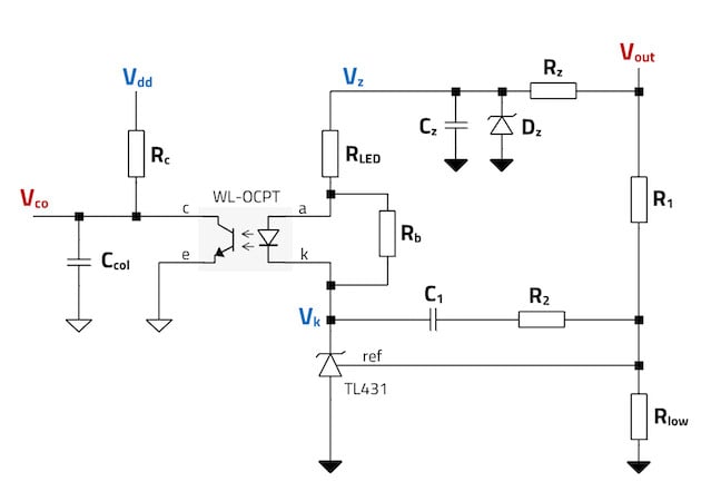
Figure 1. Optocoupler-based type-2 compensator with TL431. Image used courtesy of Bodo’s Power Systems [PDF]
The transfer function of this compensator circuit in the Laplace s-domain is as follows (Ref[4]):
\[C(s)=\frac{V_{co}(s)}{V_{out}(s)}=-G_{m}\cdot\frac{\Big(1+\frac{\omega_{z}}{s}\Big)}{\Big(1+\frac{s}{\omega_{p}}\Big)}=-\Big(\frac{R_{c}\cdot CTR}{R_{LED}}\cdot\frac{R_{2}}{R_{1}}\Big)\cdot\frac{\Big(1+\frac{1}{s\cdot R_{2}\cdot C_{1}}\Big)}{\Big(1+s\cdot R_{c}\cdot (C_{col}+C_{opto})\Big)}\,\,\,(E.1)\]
Observe how the CTR affects the term Gm (a.k.a. midband Gain), while the phototransistor parasitic capacitance (Copto) affects the pole frequency (ωP).
Selecting a WL-OCPT 817 optocoupler from the bin ‘B’ means that the DC-CTR tolerance out-of-production will be between 1.3 and 2.6 (Ref[3]), measured with a DC-bias of VCE = 5 V and ILED = 5 mA. But in the converter operating in closed loop, the compensator output voltage and, in turn, the optocoupler DC-bias point are set by operating conditions like input voltage and output current. Thus, the new CTR range for the DC-bias point representing the worst-case condition needs to be obtained.
The example design used in this article is a flyback converter with the following basic specification: Vin = 36 to 57 V, Vout = 12 V, Iout = 3 A, and Fsw = 300 kHz. The transformer used is the WEPOEH 7491195112 from Würth Elektronik, and the controller IC is the NCP12700 from Onsemi. The equivalent output capacitance is 100 µF with ESR of just a few hundred µΩ (shifting the ESR zero to the MHz range with no influence on the plant response (Ref[4])).
The compensator is designed for the worst-case condition of the control-to-output transfer function, corresponding to minimum input voltage (36 V) and full-load current (3 A) (i.e., where the right-half-plane-zero is at the lowest frequency). At this operating point, the compensator (and optocoupler) output voltage is VCO = 2.7 V (Ref[4]). With Vdd = 5 V and RC = 5 kΩ fixed by the NCP12700, then a phototransistor current of IC = 0.46 mA results.
Measuring Optocoupler CTR and Parasitic Capacitance (Copto)
The CTR at this DC-bias condition (VCO = 2.7 V and IC = 0.46 mA) can be obtained in different ways. One of them is by using the CTR vs. ILED curve provided in the WL-OCPT 817 series datasheet (Ref[3]), while another approach can be to run a SPICE simulation with the freely provided WL-OCPT SPICE models.
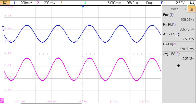
Figure 2. Optocoupler DC and AC CTR measurement (ILED – blue, IC – violet). Image used courtesy of Bodo’s Power Systems [PDF]
However, there is no more accurate approach than to measure it directly. For this, a WL-OCPT 817 sample device from bin ‘B’ with a CTR close to the average of the bin’s range at the reference test DC-bias conditions should be used (i.e., ideally CTRAV = 1.95 at VCE = 5 V, ILED = 5 mA).
In this case, the reference device used had a DC-CTR of 2.08, close to the average of the binning, and its LED and phototransistor currents at VCE = 2.7 V are shown in Figure 2, measured as voltages across 5 kΩ resistors (ILED (blue) and IC (violet)).
The DC currents are IC = 0.46 mA (i.e., 2.29 V / 5 kΩ) and ILED = 0.512 mA (i.e., 2.56 V / 5 kΩ). The ratio of the DC voltages corresponds to the DC-CTR, in this case equal to 0.9 (i.e,. 2.29 V/2.56 V).
Observe how a small amplitude, low-frequency AC sinusoidal current is also superimposed on the DC current across the LED. Here, the ratio of the measured amplitudes corresponds to the small-signal or AC-CTR, which at this operating point is 1.3 (i.e., 378 mV/285 mV).
For the DC-biasing of the optocoupler and TL431 in the compensator circuit, the DCCTR is used for relevant component calculations, whereas for control loop stability and dynamic behavior of the compensator circuit, where small amplitude AC signals are considered, the small-signal AC-CTR should be used. Note that there are some cases where both DC and AC CTR values are close enough, so that the DC-CTR can then be used as an approximation (e.g., as in Ref[4]). But this is not always the case.
With the DC and AC CTR values already known, Copto needs to be measured before advancing to the compensator design. The measured frequency response of the bin ‘B’ reference sample used, biased at VCE = 2.7 V and IC = 0.46 mA, with RC = 5 kΩ as in the compensator circuit, is shown in Figure 3.
The corner frequency is around 18 kHz, and with this, the nominal Copto can be calculated:
\[C_{opto}=\frac{1}{2\cdot\pi\cdot R_{c}\cdot \text{f}_{p\_opto}}\approx1.77nF\]
Observe how the Magnitude curve in the lower frequency range below 1 kHz is mostly ‘flat’ at a value of 2.325 dB, which corresponds to the AC-CTR of 1.3.
Compensator Design and Stability Analysis
The compensator is designed to achieve an open-loop crossover frequency of 2 kHz and a phase margin of 60º. At 2 kHz, the plant transfer function has a magnitude of 1.32 dB and a phase of -71º (Figure 4). Thus, the compensator response needs to have a magnitude of -1.32 dB and a phase of 131º at 2 kHz. For this, the following compensator component values are selected: R2 = 5.6 kΩ, C1 = 33 nF, and CCOL = 4.7 nF. The procedure followed for this calculation and for the rest of the components of the compensator circuit of Figure 1 goes beyond the scope of this article, but it is covered in detail in Ref[4].
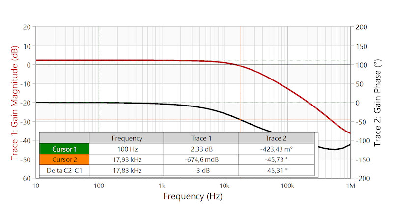
Figure 3. Frequency response of WL-OCPT 817 bin B sample. Image used courtesy of Bodo’s Power Systems [PDF]
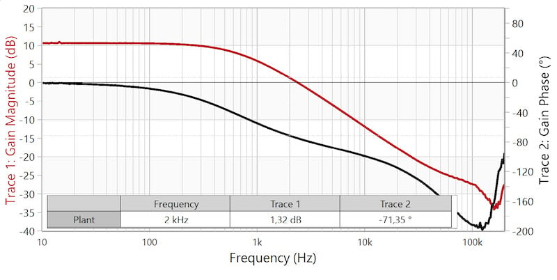
Figure 4. Plant transfer function with measured magnitude and phase at 2 kHz. Image used courtesy of Bodo’s Power Systems [PDF]
As mentioned before, the bin ‘B’ has a CTR production tolerance of around ±30%. With a nominal DC-CTR value of 0.9 for the DCbias conditions of this design, this results in a CTR range between 0.6 and 1.2. In order to experimentally assess the impact of this production tolerance on the converter stability margins, a WL-OCPT 817 device from bin ‘A’ having a DC-CTR of 0.61 and a sample from bin ‘C’ with a DC-CTR of 1.22 (both measured at VCE = 2.7 V with RC = 5 kΩ as in this design) can be used, as they are slightly above and below the estimated CTR limits of the bin ‘B’. Their measured AC-CTR values are 0.84 and 1.83 for the bin ‘A’ and bin ‘C’ samples, respectively.
Note that the CTR and Copto are directly related: a device with a higher CTR will suffer from a higher Copto for the same DC-bias condition, and vice versa. The frequency response for the bin ‘A’ and bin ‘C’ devices is also measured, obtaining corner frequencies of 24.4 kHz and 12.5 kHz, respectively.
These, in turn, correspond to Copto values of 1.3 nF for the bin ‘A’ device and 2.6 nF for the bin ‘C’ device. This capacitance variation will shift the compensator pole to lower and higher frequencies, respectively, compared to the nominal case of the bin ‘B’ sample used for the design. Observe how the bin ‘A’ sample represents the minimum expected values of CTR and Copto of the bin ‘B’, while the bin ‘C’ sample represents the maximum ones.
Figure 5 shows the measured Bode plot of the compensator transfer function for these three samples: bin ‘A’ (red), bin ‘B’ (blue), and bin ‘C’ (black). A change in the midband gain (see around 2 kHz) is clearly observed, while the variations in the pole frequency are less obvious due to the wide frequency range covered on the X-axis.
Finally, Figure 6 shows the open-loop frequency response, where a crossover frequency variation between 1.1 and 2.2 kHz can be observed. In this example, the phase margin, which determines stability, remains high between 68º and 79º, despite a rather wide variation of the optocoupler parameters.
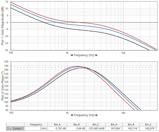
Figure 5. Measured frequency response of compensator with CTR variations of WL-OCPT 817 bin B (min (red), nom (blue), max (black)). Image used courtesy of Bodo’s Power Systems [PDF]
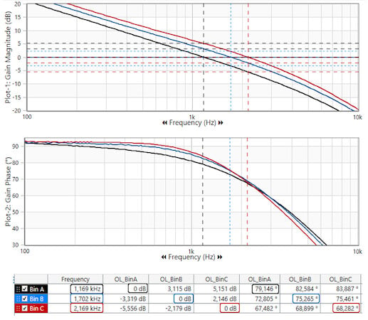
Figure 6. Measured frequency response of open-loop transfer function with CTR variations of WL-OCPT 817 bin B (min (red), nom (blue), max (black)). Image used courtesy of Bodo’s Power Systems [PDF]
In addition to this, the impact of operating temperature variations over the expected range must also be studied. Here, a thermal chamber will help to perform this evaluation experimentally with the previous samples. Another factor to consider is the optocoupler’s LED degradation with operating time, and Ref[2] provides guidance for this. However, when operating at low LED currents and not too high ambient temperatures, as in this design, the influence of the LED degradation will be negligible. For reference, the DC-DC converter prototype used for the measurements is shown in Figure 7.
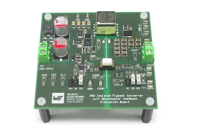
Figure 7. 30W Flyback converter prototype board. Image used courtesy of Bodo’s Power Systems [PDF]
Conclusion
Evaluating the impact of optocoupler parameter variations on the stability margin of a power supply’s feedback loop is key to ensuring reliable operation over the converter’s operating life. This article showed an example approach to do this based on real measurements, instead of simulations or calculations.
This is partly made possible by the tight CTR binning classification that Würth Elektronik provides for its WL-OCPT optocouplers.
References
[1] Application Note ANO007 – Understanding Phototransistor Optocouplers, Würth Elektronik
[2] Application Note ANO006 – Lifetime of Optocouplers, Würth Elektronik
[3] Optocoupler OCPT 817 Series, Würth Elektronik Datasheet
[4] Application Note ANP113 – Feedback loop compensation of a current-mode flyback converter with optocoupler, Würth Elektronik
This article originally appeared in Bodo’s Power Systems [PDF] magazine.