Facebook
 Google
 GitHub
 Linkedin
Using Sintering Technology to Reduce Failure Rate of High Current Thyristors
This article explores several ways to reduce degradation and early failures of power semiconductor thyristors with a semiconductor chip dia. 80 mm or more
This article explores several ways to reduce degradation and early failures of power semiconductor thyristors with a semiconductor chip dia. 80 mm or more using low-temperature sintering of silicon chips and molybdenum discs. The authors study comparative relations between VTO/rT, Rthjc, ITAV, ITSM and mounting force for options with sintering/alloying and standard cathode layer or molybdenum cathode layer with an evaporated protective interface, and select the best design to minimize the number of early failures in the field.
Leading manufacturers of power semiconductors tend to focus on the reliability of conversion equipment and its components due to growing in-service failure costs. Failure here implies a degradation failure.
Degradation failures are unavoidable since they are caused by natural aging and wear out of structure and materials. For this reason, manufacturers of power semiconductors keep improving their engineering solutions to minimize the probability of a degradation failure. For example, using sintering technology in the production of single-chip power semiconductor thyristors, diodes [1,6], and IGBT devices [2,4,5,10] helps to decrease the chance of degradation failures at the final stage of operation and improve their service life [3,4,8-10]. Minimizing degradation failures is primarily achieved by a high cycling resistance of the junction between the semiconductor chip and molybdenum disc, as well as lower junction-housing thermal resistance [3,4,6,7] leading to higher maximal surge current [1].
However, apart from degradation failures during normal operation, a customer can also experience early failures during the run-in period caused by defects unidentified by production and acceptance quality control. At the same time, carrying out the run-in period in operation conditions by the manufacturer is economically impractical. Thus, minimizing the number of early failures is only possible by reducing the probability of potentially defective devices.
A major part of power semiconductor thyristors and diodes are “low cost” products where silicon chip is joined with molybdenum disc by alloying technology with silumin soldering alloys. This process is characterized by a high dispersion of thermal resistance across the surface area caused by insufficient fusion in the weld and a higher deformation of the semiconductor chip after the joining process. This problem is especially relevant for thyristors and diodes with an area of the semiconductor chip equal or more than 50 cm2. Optimizing the joint profile between the silicon chip and molybdenum disc allows the reduction of the insufficient fusion and deformation profile. Aside from temperature profile, the amount of insufficient fusion is also affected by the roughness of the joined surfaces, quality of components cleaning, etc.
Consequently, using the sintering technology to produce power semiconductors not only reduces the number of degradation failures and improves service life, but also minimizes early failures during the run-in period.
Experimental Samples
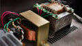
Our experimental samples were thyristors TF173-2000-18 with semiconductor chips dia. 80 mm, where silicon chip and molybdenum disc were joined by sintering and alloying technology. Each of these options had two variants of cathode layers: a standard cathode layer and a molybdenum layer with an evaporated protective interface.
The research program included the following:
- measurement of comparative deformation profiles of the semiconductor elements;
- measurement of comparative relations between on-state threshold voltage and resistance (VTO/rT) and mounting force in the range of 30 kN to 50 kN;
- measurement of comparative relations between junction-housing thermal resistance (Rthjc) and mounting force in the range of 30 kN to 50 kN;
- calculation of comparative relations between on-state current (ITAV) and mounting force in the range of 30 kN to 50 kN;
- finding values of destructive surge on-state current (ITSM).
Deformation of the Semiconductor Element
Deformation profiles are shown in Figure 1.

Figure 1. Profile of semiconductor element deformation (sintering on the left, alloying on the right)
Figure 1 demonstrates that the deformation profile for the sintered semiconductor element is much smoother than for the semiconductor element alloyed on silumin soldering alloy. The residual bend of the alloyed semiconductor element is 11 µm. The residual bend of the sintered semiconductor element is 45 µm.
Electric Properties
Relations between average values of VTO/rT, Rthjc, ITAV and mounting force are shown in Figures 2-5.

Figure 2. Relation between VTO and mounting force

Figure 3. Relation between rT and mounting force

Figure 4: Relation between Rthjc and mounting force

Figure 5: Relation between ITAV and mounting force
The graphs demonstrate that the option “Sintering, Мо layer” has the lowest values of VT0/rT (-5,8% and -11,2% respectively in comparison to the standard option, “Alloying, standard layer”). However, the option “Sintering, standard layer” has the lowest thermal resistance Rthjc (-9,7% in comparison to standard option) and the highest results of calculated average current (+12,8% in comparison to standard option). It should also be noted there is a higher relation between anode thermal resistance and mounting force for sintered options in comparison to alloyed options. Theoretically, it can be explained by the deformation of the semiconductor element when alloyed options start forming surfaces of a third or higher order that can not be completely straightened with external installation force. Meanwhile, the sintered structures are characterized by a dome-shaped surface that straightens under higher force. This is also confirmed by absolute values of anode thermal resistance that are lower for the sintered options.
From the point of view of the destructive surge current, this value is higher by 5-7% for the options “Sintering, Мо layer” and “Sintering, standard layer” in comparison to the standard option.
Conclusion
This article explored comparative relations between VTO/rT, Rthjc, ITAV, ITSM, and mounting force for options with sintering/alloying and standard cathode layer/molybdenum cathode layer with an evaporated protective interface. It was shown that in order to reduce the number of early failures encountered by a customer, it is preferable to use option “Sintering, standard layer” as the basic structural element because this option had the lowest values of thermal resistance and the highest on-state current.
About the Authors
Dmitry Titushkin works as a Research and Development Engineer at Proton-Electrotex JSC, a Russian company mainly involved in development, manufacturing and sales of bipolar power semiconductor devices — diodes and thyristors, power assemblies and IGBT modules.
Alexey Surma is head of Research and Development Center at Proton-Electrotex, a Russian company, which develops and manufactures power semiconductor diodes, thyristors, modules, heatsinks, IGBTs and power units for various electric energy converters. The company was founded and started production in 1996. As the head of R&D Center, Mr Surma is mainly responsible for the development of new technologies and products.
Alexander Stavtsev works as the Technical Director at Proton-Electrotex JSC.
Sergey Matyukhin works as an Associate Professor at the State University — Education-Science-Production Complex (EPSC) where he also acts as a docent.
References
- H. Schwarzbauer. Novel Large Area Joining Technique for Improved Power Device Performance. - IEEE Transactions on Industrial Applications, 27 (1), 1991, p. 93- 95.
- M. Knoerr, S. Kraft, A. Schletz. Reliability Assessment of Sintered Nano-Silver Die Attachment for Power Semiconductors. - IEEE Electronics Packaging Technology Conference, 12, 2010, p. 56-61.
- U. Scheuermann, P.Wiedl. Low Temperature Joining Technology-A High Reliability Alternative to Solder Contacts. - Workshop on Metal Ceramic Composites for Functional Application, Vienna, 1997, p 181-192.
- C. Göbl, P. Beckedahl, H. Braml. Low temperature sinter technology Die attachment for automotive power electronic applications. – Proc. Automotive Power Electronics, Paris ,2006.
- J. G. Bai, G.Q. Lu. Thermomechanical Reliability of Low-Temperature Sintered Silver Die Attached SiC Power Device Assembly. - IEEE Transactions on Device and Materials Reliability, 6 (3), 2006, p. 436- 441.
- A. Chernikov, A. Stavtsev, A. Surma. Features of wafer - Mo joining by sintering of silver paste for large area silicon devices. – Proc. EPE’2013, Lille, 2013
- Dmitriy Titushkin, Alexey Suma. «New ways to produce fast power thyristors» - Bodo’s Power Systems 08, 2015, p. 28- 29.
- J. Steger. With sinter-technology forward to higher reliability of power modules for automotive applications. - Power electronics europe, 2, 2012, p. 28-31.
- R. Amro, J. Lutz, J. Rudzki, M. Thoben, A, Lindeman. Double-Sided Low-Temperature Joining Technique for Power Cycling Capability at High Temperature - Proc. EPE’2005, Dresden, 2005.
- C. Göbl, J. Faltenbacher. Low temperature sinter technology Die attachment for power electronic applications. – Proc. CIPS 2010, Nuremberg ,2010.
This article originally appeared in the Bodo’s Power Systems magazine.