Facebook
 Google
 GitHub
 Linkedin
Solving Military-Avionics DC-DC Power Challenges with Modularity—Part 2
In Part 1, we covered the key standards for military and avionics power supply design. Here in Part 2, we examine managing input bus electrical overstress.
This article is published by EEPower as part of an exclusive digital content partnership with Bodo’s Power Systems.
After outlining the key standards for military and avionics power supply design in Part 1, this Part 2 turns to one of their most demanding challenges: managing input bus electrical overstress. The wide bus voltage range, transients, spikes, and undervoltage conditions all present a strict set of constraints for the power electronics designer.
Here In Part 2, we break down how overvoltages are characterized in these standards and look at practical methods to suppress them. We look at spikes and surges and explain how a transient limiter works.
Duration and Energy
When it comes to spikes and surges, it always comes back to two basic characteristics: duration and energy. What is the difference between these two and what does this mean for the design engineer?

Image used courtesy of Adobe Stock
Spikes
What is referred to as “spike” in this article is an over-voltage that lasts less than 1 ms. When the duration exceeds this value, it is common to refer to the event as a “surge.” Understanding this distinction is crucial because each kind of over-voltage requires treatment by a different device.
Typically, spike protection is expected to implement a clamping device such as a Transient Voltage Suppression (TVS) diode, a Metal Oxide Varistor (MOV), or a gas discharge tube. This is possible because the relatively short duration of spikes means they contain an amount of energy that can be handled by a single clamping component.
To select any clamping device’s protection, three parameters must be considered that will be provided by the standard: the peak voltage, the duration, and the energy or the source impedance.
Let’s take as example the injected voltage spikes described into the MIL-STD-1275F. The table 3 in part 1 of this story shows a spike with the following specifications: +/-250 V 70 µs and 200 mJ. This is referring to the envelope of the transient spike described into the standard (Figure 1 below). Over the course of the last three revisions of Mil-STD-1275, the maximum energy specified increased from 15 mJ in revisions C and D to 2000 mJ in revision E, and finally returned to 200 mJ in revision F.
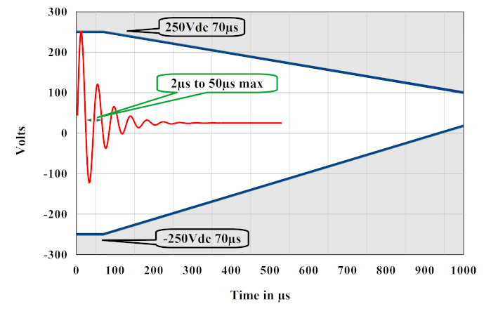
Figure 1. The graph defined into Mil-Std-1275F describes only the envelope of the spikes (blue line). The spike waveform is shown here above (red line). Image used courtesy of Bodo’s Power Systems [PDF]
We have the peak voltage, the pulse duration, and the energy—but to properly match the clamping protection to our design, one more parameter is needed: the minimum clamping voltage, which is the voltage threshold at which the device begins to conduct significant current. According to the MIL-STD-1275F standard, the most severe threat to the clamping device itself is a 100 V surge with a 50 ms duration.
To prevent damage from excessive current flow during this extended event, the protection device must begin clamping at or slightly below 100 V. We can now select a clamping device rated to trigger at 100 V and capable of withstanding 200 mJ of energy.
However, this energy is not delivered instantaneously. A reasonable assessment of the waveform (red curve) indicates that the initial, most aggressive surge—the first arch—contains less than 66 mJ of this total 200 mj energy. This first arch has extreme characteristics such as a very fast rise time of up to 50 ns (a slew rate of 5 V/ns to reach 250 V) and a minimum duration estimated at 1 µs (a half-period of 500 kHz), that is expected to be softened by the input impedance of a power supply.
Using a conservative approximation of 66 mJ dissipated over 25 µs, we can consider a 2.64 kW power and 10.56 A peak current under 250 V. With these requirements defined, we can evaluate suitable clamping devices:
- SMCJ78CA (Littelfuse)[2.1]: This device could be a candidate. Its maximum clamping voltage is 126 V at its peak pulse current of 11.9 A. While it appears to meet the current requirement, its clamping voltage is too high to protect any downstream circuitry rated for only 100 V.
- SMDJ78CA (Littelfuse)[2.2]: This is a more robust solution. With a peak current capability of 23.8 A, it provides significant margin over the calculated 10.56 A requirement. This ensures reliable operation and provides effective protection for circuits with a 100 V maximum rating.
- 5KP78CA (Littelfuse)[2.3]: If board space is not a constraint, a higher-power component like this offers maximum margin and “peace of mind.” Thanks to its vastly higher current handling (40.5 A).
Of course, these results can be revised to a lower value if the power supply input is capacitive, as the capacitive impedance can handle a non-negligible part of the spike’s energy. It is noticeable that the qualification test procedure requires a minimum of 100 spike injections applied each at a rate of one every second. Sometimes, spikes are applied between ground and plus or minus termination. In this case some safety considerations may indicate if TVS are allowed or not. Figure 2 shows the position of the spike suppressor at the front side of the power architecture.
The clamping protection devices function by overloading the spike source to maximize the voltage drop across its internal impedance. Consequently, a TVS diode, MOV, or gas tube will be ineffective if the spike source exhibits zero internal impedance. However, clamping protection is useless in some cases, as transient spike voltages generated by a high-impedance source can be attenuated simply with a capacitor or LC filter.
For example, consider the DO160G Section 17 specification: a 600 V/10 µs spike into a 50 Ω source impedance. When this spike is applied to any GAIA converter filter in the FGDS series, the 600 V transient is reduced to just a few volts, well within the tolerance of the downstream converter. As an example, the FGDS-2A-50V, when subjected to this 600 V spike, exhibits a transient impedance of approximately 0.7 Ω, limiting its output voltage rise to no more than 35 V (Figure 3).
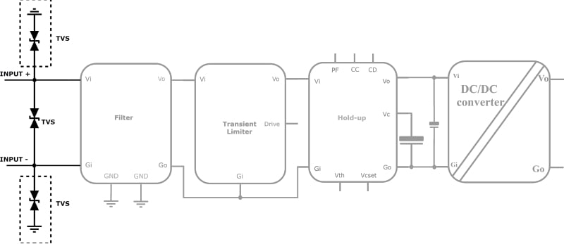
Figure 2. The spike protections such as TVS are connected between input+ and input- of a power architecture, and can also be populated across inputs and ground. Image used courtesy of Bodo’s Power Systems [PDF]
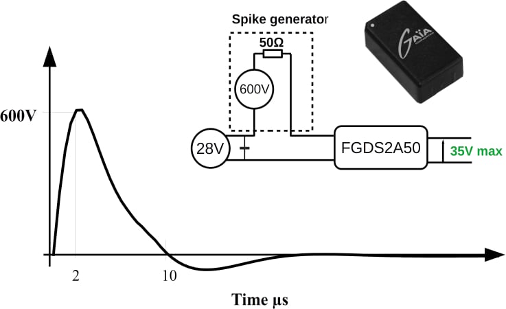
Figure 3. Thanks to the 50 Ω internal impedance, the DO160 600V spike can be dampened directly by a FGDS-2A-50V EMI filter. Image used courtesy of Bodo’s Power Systems [PDF]
Surges
When clamping a surge transient voltage, relying on overloading the surge source to cause a voltage drop is no longer viable because the source impedance is usually very low or the surge duration is too long. In such cases, the energy contained in the surge is too high for a single clamping component that will be damaged.
The most common approach for handling transient surges is to insert a series element into the input bus that introduces a voltage drop when input voltage reaches a given level. This method imply the transient protection needs to pass-through the total current drawn by the downstream converter. Figure 4 presents a basic example of a discrete P-MOSFET-based transient voltage limiter. Choosing a discrete solution over a ready-to-use COTS-based modular approach introduces three key challenges:
- Safe Operating Area (SOA) Compliance: The MOSFET will operate in its resistive mode during the surge event. This requires the designer to verify that the selected transistor operates within its SOA. Since the SOA is typically specified at 25 °C, the designer must extrapolate the data across the full temperature range of its reliability application, from -40 °C to 105 °C.
- P-MOSFET choice: While many P-MOSFETs are available for low-power applications (below 50–80 W), higher power projects typically require N-MOSFETs. Implementing a surge limiter with an N-MOSFET using discrete components leads to a much more complex design.
- Thermal Management: Managing heat generated by the MOSFET during clamping adds significant design complexity and requires complex thermal calculations.
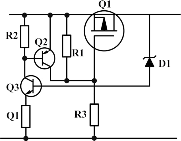
Figure 4. A series element such as the Q1 of this transient limiter allows to handle long lasting overvoltage. Image used courtesy of Bodo’s Power Systems [PDF]
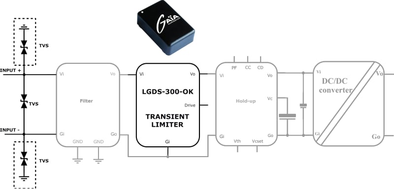
Figure 5. In this power supply architecture, the LGD-300-OK transient limiter, placed after the EMI filter that allows the surge to pass, limits any surge from 50 to 100 VDC to a lower voltage acceptable for the converters, while reducing the inrush current. Image used courtesy of Bodo’s Power Systems [PDF]
Although driving circuits for N-MOSFET-based transient limiters are now commercially available, ensuring Safe Operating Area (SOA) compliance across temperature ranges, thermal management, and other military qualifications remains challenging for designers pursuing discrete solutions. Adopting a modular approach with Commercial Off-The-Shelf (COTS) products significantly simplifies the designer’s task and accelerates development timelines for any project. GAIA Converter offers transient limiters with voltage capabilities from 80 V to 202 V, meeting most industry standards.
These modules feature output clamping voltages compatible with a wide range of DC/ DC converters and power ratings from 50 W to 600 W. Housed in encapsulated metallic cases, these board-mounted modules are fully qualified for military and avionic applications. Designed for high reliability, they achieve very high Mean Time Between Failure (MTBF) figures.
Some variants integrate additional functions such as reverse polarity protection, inrush current limiting, hold-up support, and (in the latest models) integrated EMC filtering. An overview of GAIA Converter’s COTS transient limiters is provided in Table 1.
Table 1. From 50 to 600 W, the GAIA Converter transient limiters come in potted metallic case board-mounted modules, enabling compliance with the main defense and avionic standards.
|
||||||||||||||||||||||||||||||||||||||||||||||||||||||||
Avoiding Transient Limiter
Just as effective input filtering can eliminate the need for spike protection by dampening overvoltage below a DC/DC converter’s maximum limit, high-performance DC/DC converters with wide input ranges may similarly obviate surge protection devices. For example, GAIA Converter’s MGDD-80-N-E (80 W, 9–80 VDC input) and MGDS-100-M-C (100 W, 10–100 VDC input) can withstand transient inputs up to 80 VDC (per DO-160) and 100 VDC (per MIL-STD-1275), respectively, without damage.
This resilience stems from their use of current-mode control in the regulation loop. Unlike converters using voltage-mode control—which only responds to input surges after the output voltage rises, risking brief output overshoot—this current-mode control proactively monitors input current and adjusts regulation, preventing output disturbances.
What’s Next?
As established in Part 1 of this series, military and avionic standards define the maximum levels of electromagnetic interference (EMI) alongside surges and spikes that a power supply must comply with. For switching-mode power supplies (SMPS), these disturbances also represent a significant source of emissions, creating an additional design challenge. The upcoming Part 3 of this story will break down the various modes of electromagnetic interference (EMI) propagation and describe methods to contain it, with a focus on using EMC filters.
References
[2.1] Littelfuse SMCJ78CA datasheet
[2.2] Littelfuse SMDJ78CA datasheet
[2.3] Littelfuse 5KP78CA datasheet
This article originally appeared in Bodo’s Power Systems [PDF] magazine.