Facebook
 Google
 GitHub
 Linkedin
Isolation Technology Under High dv/dt Stress
Isolation technologies respond differently to fast voltage changes. This article examines how capacitive, magnetic, and optical isolation perform when they face high dv/dt stress.
When power stages switch fast, isolation barriers face sudden voltage changes that show how each technology deals with stress. The barrier’s design affects how much transient energy gets through, which impacts noise and long-term reliability. Picking the wrong isolation type can quietly reduce insulation performance, shorten its life, and make it less reliable.
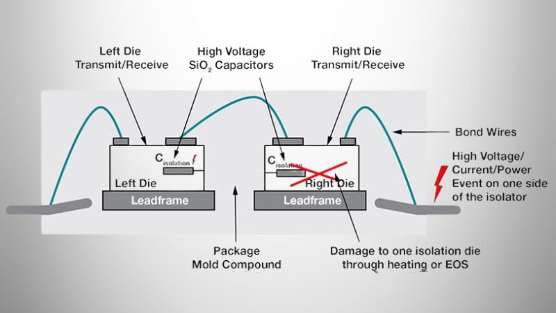
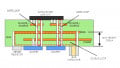
Figure 1. High-voltage transients couple across the isolation capacitance, creating an imbalance and localized heating that can damage one side of the isolator. Image used courtesy of Texas Instruments
Capacitance Isolation Under Fast Transients
In capacitive isolation, signals move through the electric field in the dielectric layer between closely spaced conductors without using magnetic or optical methods. Since the path is capacitive, a high dv/dt across the barrier creates a displacement current. This current shifts ground potentials, so while the isolator sends signals, it also lets some transient energy reach the secondary side.
Since the signal path is mainly capacitive, a fast voltage change across the barrier creates a displacement current that disturbs the ground potential on the secondary side. The equation below shows how to measure this effect.
$$I_{cm} = C_{iso} \times \frac{dv}{dt}$$
This displacement current occurs due to the capacitive design, even if the dielectric material is high quality. You can calculate the total charge injected during each switching event and the power lost across the barrier using the equations below.
$$Q_{injected} = C_{iso} \times \Delta V$$
$$P_{avg} = C_{iso} \times V^2 \times f_{sw}$$
As switching frequency goes up, power loss across the barrier also rises. This leads to higher average power loss and less thermal margin, which speeds up dielectric wear. For example, with an 800 V SiC inverter, 5 pF isolation capacitance, 100 kV/μs dv/dt, 8 ns rise time, and 100 kHz switching frequency, the peak common-mode current can reach 500 mA. This is enough to disrupt the drive logic.
$$I_{cm} = (5 \times 10^{-12}) \times \frac{100 \times 10^3}{10^{-6}} = 0.5 \text{ A} = 500 \text{ mA}$$
The resultant charge per transition can be evaluated by:
$$Q = (5 \times 10^{-12}) \times 800 = 4 \text{ nC}$$
We can then calculate the average power dissipated in the barrier using:
$$P_{avg} = (5 \times 10^{-12}) \times (800^2) \times (100 \times 10^3) = 0.32 \text{ W} = 320 \text{ mW}$$
A steady dielectric power loss of 320 mW is a big thermal load for a compact IC. You need to consider this when estimating junction temperature, since it can directly weaken the isolation barrier under high dv/dt conditions.
When the displacement current crosses the isolation barrier to the secondary side, it has to flow back through the ground path, which is not ideal. If this return path has parasitic inductance, like 10 nH (a typical value for a PCB trace a few centimeters long), a rapid change in current can cause a voltage spike.
$$V = L_{return} \times \frac{di}{dt}$$
With high dv/dt, di/dt can get very large, creating ground spikes of hundreds of millivolts that can disrupt the drive logic. Since typical logic thresholds are between 400 and 800 mV, these spikes can go past the margin, upset the ground reference, cause false switching, and eventually lead to CMTI failure.
One benefit of this isolation method is that it allows fast switching with little delay and works well for compact IC designs. However, capacitive isolation lets common-mode transients through, making it sensitive to noise in high dv/dt situations. Repeated transient currents can also slowly damage the insulation.
Magnetic Isolation (Transformer-Based)
Magnetic isolators use a transformer to send signals through a changing magnetic field. Current in the primary winding creates a signal in the secondary without a direct electrical connection. While transformers are meant to block DC and common-mode noise, real designs have parasitic capacitance between windings, which can let high-frequency transients through.
In an ideal transformer isolator, no voltage or current crosses the barrier. In a real transformer-based magnetic isolator, though, two parasitic effects create dv/dt-sensitive leakage paths.
Mechanism 1 - Interwinding Capacitance
The interwinding capacitance (Cw) between the secondary and primary windings, arranged in an overlapping winding pattern, allows displacement current flow across the barrier, as in a capacitive isolator.
$$I_{leak} = C_w \times \frac{dv}{dt}$$
Since interwinding capacitance depends on geometry, it is estimated using a parallel plate model from a simple winding stack. This looks at the overlapping area (Aoverlap) of the secondary and primary windings and the interlayer insulation thickness (dinsulation). For example, a coreless on-chip transformer with a 200 μm by 200 μm winding overlap and a 20 μm polyimide insulation layer with a relative permittivity (εr) of 3.4 gives about 0.6 pF capacitance. This is usually less than the 5 pF of a capacitive isolator, which is why magnetic isolators often have higher CMTI ratings, since the displacement current is smaller by design.
$$C_w = \varepsilon_0 \times \varepsilon_r \times\frac{A_{overlap}}{d_{insulation}}$$
$$C_w = (8.85 \times 10^{-12}) \times 3.4 \times\frac{4 \times 10^{-8}}{20 \times 10^{-6}}$$
Mechanism 2- Leakage Inductance Voltage
Leakage inductance (Llk) comes from magnetic flux that does not couple between the primary and secondary windings, causing a voltage drop during fast current changes. In gate drive transformers, where current charges the power device’s gate capacitance, this inductive voltage opposes the drive voltage at the start of a transient. As a result, a large portion of the input voltage is briefly lost across the leakage inductance, slowing current buildup and lowering the effective secondary voltage.
$$V_{leak} = L_{lk} \times \frac{di}{dt}$$
This appears as a temporary voltage error that disappears once the current stabilizes, making leakage inductance a major challenge in transformer-coupled isolators, even more than common-mode injection. Interwinding capacitance, on the other hand, is the main cause of common-mode coupling and gives magnetic isolators better rejection of common-mode transients than capacitive isolators.
When designed well, magnetic isolation can handle moderate-to-high dv/dt and offers a good balance between speed and noise immunity. However, its performance depends greatly on transformer design and PCB layout, since winding-induced parasitic capacitance can create a dv/dt-sensitive leakage path. If not done consistently, magnetic isolation can act unpredictably across different units.
Optical (Fiber Optocoupler) Isolation
Optical isolation uses an LED and a photodetector separated by insulation to send signals with light, with no direct electrical connection between input and output. Since there is no conductive or capacitive path, transient coupling is almost eliminated, especially if the design keeps barrier capacitance low. This makes optical isolators naturally resistant to common-mode disturbances, even at very high dv/dt.
One drawback is that this method usually switches more slowly, especially as the optocoupler's LED ages, which lowers output and performance. The delay in signal passing through the barrier depends on the LED's lifetime (τLED) and the photodetector's RC time constant (τdet).
The total delay can therefore be evaluated as:
$$t_{pd} \approx \tau_{LED} + R_{det} \times C_{det} $$
You can find the maximum signal speed using the equation below. More delay means lower bandwidth and a slower response.
$$f_{max} \approx \frac{1}{2 \times t_{pd}}$$
Common mode transient immunity (CMTI) sets the highest dv/dt an isolator can handle without causing false output signals. This research shows how well the isolator keeps signal accuracy during fast common-mode transients, but it does not measure insulation voltage rating. In practice, CMTI specs are based on ideal lab tests with minimal parasitics and standard waveforms, which rarely match real system conditions.
Factors like PCB parasitics and external noise can lower CMTI well below the value shown in the datasheet. What looks good on paper may become borderline in a high-speed, high-voltage design.
Qualitative Comparison Across Technologies
All three technologies differ under the same conditions: an 800 V bus, 100 kV/µs dv/dt, 8ns rise time, and 100 kHz switching frequency. The findings reveal insights that a simple qualitative description cannot capture.
Table 1. Qualitative comparison across different isolation technologies.
| Parameter | Capacitive | Magnetic | Optical |
| Barrier Capacitance | 5pF | 1.5pF | 1.0pF |
| Peak Icm | 500mA | 150mA | 100mA |
| Charge per Transition | 4nC | 1.2nC | 0.8nC |
| Avg. Barrier Dissipation | 320mW | 96mW | 64mW |
| Bandwidth Limitation | Encoding delay | Leakage inductance | LED + detector RC |
| CMTI sensitivity | High | Moderate-geometry dependent | Low-filtered by detector RC |
Even though all three technologies use the same basic displacement current equation, their performance changes based on barrier capacitance and how well they suppress induced current. Optical isolation lowers capacitance by removing electric coupling, and magnetic isolation reduces it by separating winding geometry. Capacitive isolation has higher capacitance but uses on-chip differential signaling to help. Choosing between them means matching the right capacitance and recovery setup to the dv/dt and CMTI needs of your application.
Isolation Selection Guideline for High dv/dt System
The isolation barrier affects how transients couple and impact signal integrity, so picking the right technology means matching the device’s behavior to the system’s electrical stress profile.
Table 2. Practical recommendations for isolation types based on application needs
| Isolation type | Best use case |
| Capacitive | Ideal for low-to-moderate dv/dt with high speed, requiring careful layout to control noise. |
| Magnetic | Balanced for moderate to high dv/dt, offering good immunity and speed, but performance varies with design. |
| Optical | Best for extreme dv/dt or high voltage settings where reliability and noise regulations trump speed. |
Key things to consider are dv/dt size, switching frequency (which affects how often the insulation faces stress), and operating voltage (which sets the basic insulation needs). These factors help you decide whether to focus on immunity, speed, or durability.