Facebook
 Google
 GitHub
 Linkedin
Improving Voltage Regulation in a Buck Converter With Isolated Output
Learn about incorporating cost-effective, non-regulated isolated outputs into buck converters for below 15 W. We explore the parameters affecting these outputs, along with design directions.
This article is published by EEPower as part of an exclusive digital content partnership with Bodo’s Power Systems.
The buck converter is arguably the most ubiquitous switching power supply topology found in low power systems, providing an output voltage which is lower than the input voltage. Although in its standard form the input and output stages are not galvanically isolated, the topology lends itself well to the addition of one or more galvanically-isolated voltage rails, as required in applications like isolated communication interfaces and gate driver systems.
Here, the buck solution represents a simple and cost-effective alternative to other topologies like flyback or push-pull converters, especially for low power levels below 15 W. However, unlike its primary nonisolated output, the added ‘secondary’ voltage rails are not directly regulated. Therefore, appropriate design measures are required to prevent them from deviating substantially from their target levels over the full range of operating conditions.
Starting with an analysis of the topology and its operation, this article identifies the factors affecting the isolated/secondary output voltage and provides design guidance to minimize its variation, all supported by real measurements.
Image used courtesy of Adobe Stock
Adding Isolated Outputs to a Buck Converter
The power stage of a synchronous buck converter is shown in Figure 1, highlighted in grey. Considering ‘ideal’ components, the dutycycle (D) of the PWM signal driving the control transistor (Q1) sets the converter output voltage (VOP), as follows:
VOP=D∙VIN (E.1)
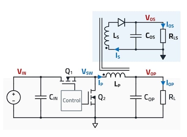
Figure 1. Schematic of a buck converter with an additional isolated output. Image used courtesy of Bodo’s Power Systems [PDF]
Regarding the inductor (L1), the voltage appearing across its terminals during the time Q1 conducts (∆tON) corresponds to the difference between input and output voltages:
VL1_ON=VIN-VOP (E.2)
In most applications, the input voltage is not fixed, but varies within a set range, and so will the voltage across the inductor during the on-time. During Q1 off-time (∆tOFF), the voltage across the inductor changes polarity and equals the output voltage in absolute value (ignoring parasitic voltage drops):
VL1_OFF=-VOP (E.3)
Unlike the input voltage, the output voltage is kept fixed in steadystate operation by a closed feedback control loop, and based on E.3, so is the inductor voltage during ∆tOFF. Thus, if an additional winding (L2) is added, magnetically coupled to L1 and with the same number of turns, then by transformer action, VOP will also appear across L2 during the off-time. By adding a peak rectifier circuit (diode and capacitor) to the second winding (secondary) as highlighted in blue in Figure 1, the diode will be forward-biased only during ∆tOFF, and VOP will also appear across the secondary load (RLS) (ignoring D1 voltage drop).
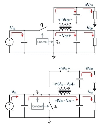
Figure 2. Equivalent circuit during Q1 on-time (bottom) and Q1 off-time (top). Image used courtesy of Bodo’s Power Systems [PDF]
The secondary/isolated output voltage is set as:
VOS = n · VOP (E.4)
Where ‘n’ is the turns ratio between secondary and primary windings:
\[n=\frac{N_{OS}}{N_{OP}}=\frac{Turns\,secondary\,winding}{Turns\,primary\,winding}\,\,\,(E.5)\]
Note how VOS can be set higher or lower than VOP by simply adjusting the turns-ratio of the coupled windings.
Figure 3 shows measured waveforms of the primary winding current (IP - violet), secondary winding current (IS - gold) and switchnode (VSW - blue) for the following specification: VOP = 5 V, D = 0.5, IOP = 0.1 A, IOS = 0.3 A, FSW = 350 kHz and using a 22 µH coupled inductor with n=1. During ∆tON, IS is zero and the primary winding current rises with a mostly 1st order slope as in a standard buck converter. Net energy is stored in the magnetic core airgap and in COP, while on the secondary side, COS supplies RLS.
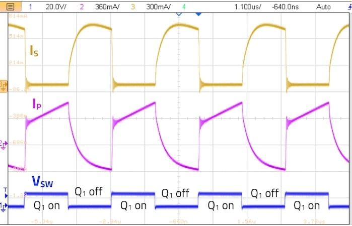
Figure 3. Measured waveforms of a buck converter with additional isolated output. Image used courtesy of Bodo’s Power Systems [PDF]
During ∆tOFF, D1 conducts and energy (previously stored during the on-time) is transferred now from the primary to the secondary side. Part of it comes from the magnetic field of the coupled inductor, while the rest was stored in the electric field of the primary output capacitor (COP). As ‘transformer action’ takes place, there is current ‘reflection’ on the primary and secondary windings. The waveshape of the windings’ currents during the off-time depends on converter operating conditions (especially the duration of the off-time window) as well as component parasitics, so it can differ from those of Figure 3 for a different specification and component selection from those considered in this example. An analysis on this goes beyond the scope of this article, but Ref[1] can be consulted for more details.
Analysis of Isolated Output Voltage Variation
Unlike VOP, which is tightly regulated by the buck converter control system, VOS is only ‘indirectly’ regulated. In the case of ideal components without parasitic elements, VOS would be a perfectly scaled version of VOP. But in reality, the voltage drops across components’ parasitic elements, as well as operating conditions like primary and secondary load currents, will all determine the final output voltage appearing across the secondary load.
When analyzing VOS regulation, the off-time interval, where energy is transferred from primary to secondary, must be considered. Figure 4 (top) shows the equivalent circuit during ∆tOFF with n=1 and the main components’ parasitic elements. These are the on-resistance of the low-side MOSFET (RDS), the primary winding resistance (RP), the secondary winding resistance (RS) and the transformer leakage inductance (Lk), referred to the secondary side. In addition, the non-linear forward voltage drop across the diode (Vf) is also included, as it has a big influence on VOS.
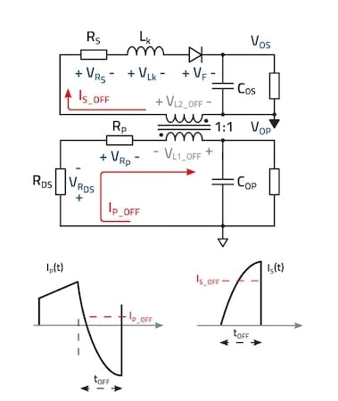
Figure 4. Equivalent circuit and current waveforms during off-time. Image used courtesy of Bodo’s Power Systems [PDF]
The average voltage drops during ∆tOFF across these elements will determine the resulting voltage on the isolated output, as follows:
VOS = VOP + VRDS + VRP - Vf - VLk_off - VRS (E.6)
For the calculation, the average current levels during the off-time on the primary (IP_OFF) and secondary (IS_OFF) windings are considered (Figure 4 (bottom)), calculated as:
\[I_{P\_OFF}=I_{OP}-\frac{D}{1-D}\cdot n\cdot I_{OS}\,\,\,(E.7)\]
\[I_{S\_OFF}=\frac{I_{OS}}{1-D}\,\,\,(E.8)\]
The individual voltage drops accross the parasitic resistive elements are then:
\[V=_{R_{DS}}=I_{P\_OFF}\cdot R_{DS}\,\,\,(E.9)\]
\[V_{R_{P}}=I_{P\_OFF}\cdot R_{P}\,\,\,(E.10)\]
\[V_{R_{S}}=I_{S\_OFF}\cdot R_{S}\,\,\,(E.11)\]
Note from E.8 how IS_OFF is always positive, so the voltage drops on the secondary side will always cause a reduction of VOS from the reflected voltage across the secondary winding during the offtime (VL2_OFF). In contrast to this, for a set duty-cycle, IP_OFF may be positive or negative depending on how the primary and secondary load currents compare (E.7). If IP_OFF is positive, the resistive voltage drops on the primary side will make the voltage across the primary winding (VL1_OFF) (which is reflected to the secondary winding scaled by ‘n’) to be higher than VOP. This may help to offset the effect of the voltage drops on the secondary side, reducing VOS deviation from its target level.
Regarding the output diode, its average forward voltage during the off-time can be directly obtained from the I-V curve given in its datasheet, as follows:
Vf = VD (@ IS_OFF) (E.12)
Of all the parasitic voltage drops happening during ∆tOFF, the most complex to calculate accurately is the one related to the leakage inductance. However, an approximation can be made and an expression obtained which helps to gain a qualitative understanding into its dependence upon other parameters.
The instantaneous voltage across the leakage inductance is:
\[V_{L_{k}}(t)=L_{k}\cdot\frac{di_{S\_OFF}(t)}{dt}\,\,\,(E.13)\]
Its average voltage drop during the off-time is approximated as follows:
\[V_{L_{k}\_OFF}\approx L_{k}\cdot\frac{\Delta I_{OFF}}{\Delta t_{OFF}}\,\,\,(E.14)\]
In E.14, ∆IOFF is the difference of the secondary winding current between start and end of the off-time window.
Considering a secondary winding current waveform increasing with a mostly 1st order slope during the off-time (valid for cases with very short ∆tOFF, high LK and/or high IOS), the following approximation can be made:
\[V_{L_{k}\_OFF}\approx L_{k}\cdot\frac{2\cdot I_{OS}\cdot F_{SW}}{(1-D)^{2}}\,\,\,(E.15)\]
The result in E.15 shows that the net voltage drop across the leakage inductance during the off-time increases with the isolated load current, the duty cycle, the switching frequency and the leakage inductance value itself. Observe how this is the only voltage drop affected by the switching frequency.
Design Guidelines
Based on this analysis, the following design guidelines should be considered to minimize deviations of the isolated output voltage from its target level:
- Low switching frequency
- Low duty-cycle
- Low conduction resistance of Q1
- Low winding resistances of coupled inductor
- Low leakage inductance (i.e. high coupling factor) of coupled inductor
- Low forward voltage of output diode (i.e. Schottky type)
From the above considerations, a low switching frequency and proper diode and coupled inductor selection are the ones that the designer can control more easily. If the non-isolated output is not used and the input voltage range is not very wide, then the dutycycle can also be freely set to a low value. In contrast, the options for RDS are more limited, as in this topology with such low output power levels, a small range of converter ICs with integrated transistors are typically used to keep the solution size and cost low.
Experimental Results
To confirm the above design guidelines, measurements on a real converter prototype are performed.
In Figure 5, experimental results show the negative effect of a higher switching frequency on the isolated output voltage for the following specification: VOP = 5 V, IOP = 0.4 A, D = 0.5 and L = 22 µH (DPC-HV 7448841220). Here, measurements for switching frequencies of 200 kHz and 800 kHz are compared and as expected, VOS remains closer to the target level when operating at a lower switching frequency, as the voltage drop across the leakage inductance is lower.
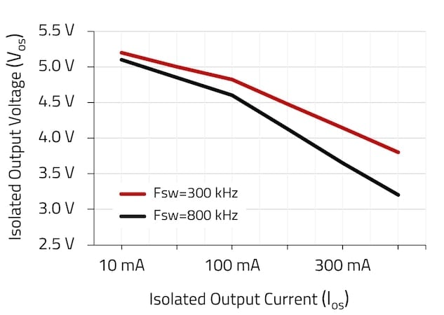
Figure 5. VOS vs. IOS at switching frequency (FSW). Image used courtesy of Bodo’s Power Systems [PDF]
In Figure 6, the measured variation of VOS with isolated load current at low and high duty-cycles of 20% and 80% is shown for the basic specification with VOP = 5 V, IOP = 0.4 A, FSW = 300 kHz and L = 22 µH (TDC-HV 76889440220). As anticipated, a lower duty-cycle results in a lower deviation of the isolated output voltage.
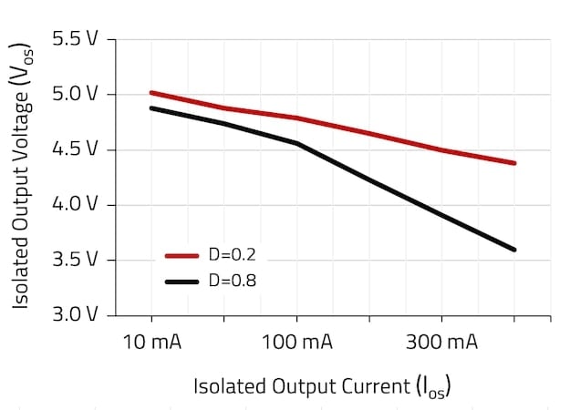
Figure 6. VOS vs. IOS at duty-cycle (D). Image used courtesy of Bodo’s Power Systems [PDF]
Regarding the influence of circuit components, the forward voltage of the output diode does not vary much with load current, as opposed to the voltage drop caused by the leakage inductance of the coupled inductor. The WE-MCRI 1090 coupled inductor series from Würth Elektronik feature variants with high and low leakage inductances, targeting different applications.
For each magnetizing inductance offered, all parameters other than the leakage inductance are kept equal in both variants, allowing for a direct comparison of the impact of the coupling factor in the circuit. Considering the following specification: VOP = 5 V, I OP = 0.1 A, D = 0.42, FSW = 300 kHz, results using WE-MCRI with L = 22 µH and coupling factor variants of 0.98 and 0.76, equivalent to leakage inductances of 0.45 µH and 5.6 µH, are compared in Figure 7.
Observe how the ‘high-leakage’ coupled inductor is unusable in this topology: with only 150 mA of load current, the output voltage has already dropped more than 2.5 V, compared to only 0.2 V for the ‘low-leakage’ part.
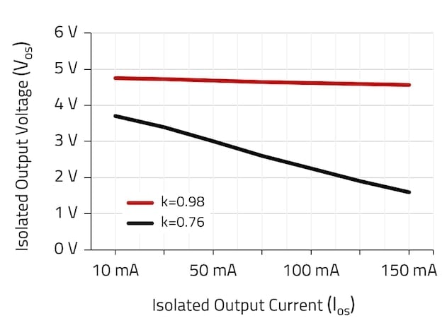
Figure 7. VOS vs. IOS at coupling factor (k). Image used courtesy of Bodo’s Power Systems [PDF]
While a high leakage inductance can be of advantage in some converters, like the SEPIC (Ref[2]), in the case of the buck with isolated output, a low leakage inductance is essential for correct operation.
Conclusion
Understanding the elements affecting the secondary output voltage(s) and designing accordingly to minimize their influence is key when designing a buck converter with isolated output(s). Parameters like the switching frequency and duty-cycle as well as the optimal selection of the output diode and coupled inductor all play a key role in this, as it has been shown in this article.
As a further read, Würth Elektronik’s ANP017 application note (Ref[1]) provides a detailed analysis of the topology, a step-by-step design example as well as alternative solutions to improve the regulation of the isolated output voltage, helping to gain a deeper insight into the operation and important design considerations of this topology.
References
[1] Application Note ANP017 – Designing buck converters with isolated outputs, Würth Elektronik
[2] Application Note ANP135 – The SEPIC with coupled and uncoupled inductors, Würth Elektronik
About the Author

Eleazar Falco. Image used courtesy of Bodo’s Power Systems [PDF]
Eleazar Falco holds a BSEE equivalent from the University of Elche (Spain). After graduation, he worked in the electronics hardware development of various home appliances and electronic products in the United Kingdom, focusing on analog circuits, power supply design, and motor control. Since 2018, Eleazar is an Application Engineer at Würth Elektronik in Germany, where he supports different product areas with a focus on power electronics applications.
This article originally appeared in Bodo’s Power Systems [PDF] magazine.