Facebook
 Google
 GitHub
 Linkedin
Solving Military-Avionics DC-DC Power Challenges with Modularity—Part 3
In Part 3 of this series, we look at how embedding a boost converter within a board-mounted module reduces the required capacitor value for a given hold-up time.
This article is published by EEPower as part of an exclusive digital content partnership with Bodo’s Power Systems.
Following our exploration of military standards and practical transient suppression, we now turn to a common challenge in switch-mode power supply (SMPS) design: containing conducted noise. In this article, we will explore conducted noise paths and filtering techniques.
Traditionally, managing bus interruptions has relied on large bulk capacitors to maintain energy on the primary side. In this third part of the series, we examine how GAIA-converter’s approach—embedding a boost converter within a board-mounted module—reduces the required capacitor value for a given hold-up time.
Propagation Modes
DC-DC converters, as switch-mode power supplies, generate conducted noise on their input and output leads. This noise appears as an alternating current waveform superimposed on the DC current, comprising multiple frequency harmonics. These harmonics originate from switching components (e.g., MOSFETs and rectifying diodes) that, when combined with parasitic capacitance or inductance, form high-frequency resonant circuits during transient operation. Two distinct propagation modes exist, each requiring specific mitigation techniques for DM noise and CM noise:
Differential Mode (DM) Noise: Current flows between the positive lead and its return path (negative lead). This noise is relatively straightforward to suppress, typically requiring only a basic LC filter with ~40 dB/decade attenuation to meet compliance limits.
Common Mode (CM) Noise is more challenging to eliminate, CM noise flows simultaneously through both positive and negative leads, returning via earth ground. It propagates through parasitic capacitances (e.g., across isolation barriers or chassis connections), inducing AC voltages along its path. CM noise arises from high dV/ dt switching transitions and typically occupies higher frequencies.
For DO-160 and MIL-STD-461, Limits are specified in dBµA, where:
\[0_{(dB\mu A)}=1_{(\mu A)}\\I_{(\mu A)}=10^{(I_{_{(dB\mu A)}}/20)}\]
Figure 1. To convert a current in dBµA to its value in µA, the reverse logarithm needs to be used.
\[0\,dB\mu A\equiv34\,dB\mu V\,thus:\\dB\mu V=dB\mu A+34dB\mu V\]
Figure 2. By adding 34 to a value in dBµA, we convert it to dBµV in a 50 Ω system.
Or with the Equivalent limits in dBµV (for 50 Ω systems):
Measurements use a Line Impedance Stabilization Network (LISN) inserted between the D.U.T (device under test) input and the lab power supply. The LISN Isolates the test circuit from lab power supply interference and provides a standardized 50 Ω test port for spectrum analyzer connection.
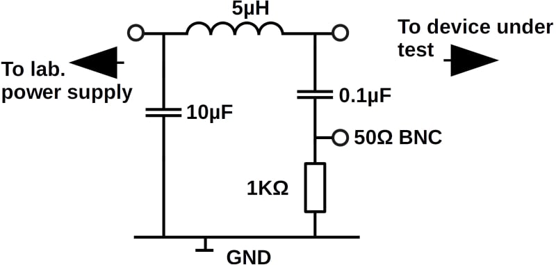
Figure 3. The LISN defined in the DO-160 standard allows isolating the lab power supply and offers a normalized source impedance for testing. Image used courtesy of Bodo’s Power Systems [PDF]
Designing Filters with Discrete Components or Using COTS
The first method to reduce common-mode noise in isolated DC-DC converters consists of placing capacitors across the isolation barrier. If the capacitors placed between the input and output pins have a value significantly higher than the few picofarads of the isolation barrier itself, they will drastically reduce the impedance of the barrier for high-frequency noise currents, thereby lowering the developed voltage.
If a chassis ground is available, it can be even more efficient to place four capacitors between the hot points and the chassis, as shown in Figure 4. To reach the lowest impedance, the best choice is to connect the common-mode capacitors as close as possible to the converter pins and the ground plane, minimizing any access inductance that could create uncontrolled resonances.
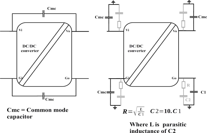
Figure 4. Common mode capacitors can be placed across primary/secondary isolation, or across input and output pins and chassis. Image used courtesy of Bodo’s Power Systems [PDF]
In some cases, a snubbing circuit may be placed in parallel with the common-mode capacitor to further reduce total impedance at the capacitor’s self-resonance frequency (also shown in Figure 4). Fortunately, most SMD chip capacitors have self-resonance frequencies high enough to avoid overlapping with the predominant harmonics of common-mode noise from typical SMPS designs, meaning this snubbing circuit can often be omitted.
When it comes to discrete filters, design might seem straightforward as they often consist of only passive components. Typically, the design starts with choosing an LC filter, where the component selection depends on the DC-DC converter’s switching frequency. However, the engineer must carefully consider several parameters:
- What should be the quality factor (Q) of the filter?
- How can potential over-voltages from surges be damped?
- How can the inrush current, due to internal capacitors, be limited?
In most cases, the filter will also include one or more common-mode inductors to further reduce the common-mode noise. While selecting a standard market-available inductor is the simplest option, it often results in an oversized component. This happens because choosing an inductor with the needed inductance often restricts the available options to parts rated for much higher maximum currents than needed, resulting in unnecessarily large form factors.
An optimized solution is to build a custom common-mode inductor. A common-mode inductor essentially consists of a ferrite core with two windings in the same direction. For differential-mode currents (currents flowing in opposite directions), the magnetic fluxes cancel each other out, and the core presents minimal impedance. For common-mode currents (currents flowing in the same direction), the magnetic fluxes add up, maximizing impedance.
The main advantage of building a custom common-mode inductor is the ability to select a core with a saturation level much lower than that needed for DC current, because differential-mode fluxes cancel each other. However, designing a custom inductor requires skillful calculation, thorough qualification, and significant time investment.GAIA has undertaken this task, developing over the past 25 years a complete range of passive filters directly matched to their DC-DC converters, ensuring full EMI compliance.
These filters are optimized for form factor, inrush current limitation, and have been qualified for military and aerospace applications. The GAIA filters series ranges from 2 A, 50 V (FGDS2A50V) to 35 A, 100 V (FGDS35A100V), enabling the design of power supplies from 50 W to 500 W. The entire range operates from -55 °C to 105 °C and offers a high MTBF of 8 to 27 million hours.
Hold-up Function: Maintaining Power Integrity During Bus Interruptions
When it comes to power source transfers, the DO160G standard is clear: equipment must continue to operate despite short interruptions—up to 200 ms for category A, 50 ms for category B, and up to 1 s for categories D and Z. Similarly, ABD100 outlines comparable requirements. On the military side, MIL-STD-704 accepts a bus voltage drop to 0 V for up to 7 s, but only demands that equipment survives without damage, not necessarily without interruption.
To meet these stringent requirements, one of the simplest and most effective solutions is to use a tank capacitor placed ahead of the DC-DC converter. Aluminum capacitors—or equivalent tantalum capacitors [3.1]—are typically used. These capacitors act as a reservoir during a bus dropout. However, some precautions must be taken. Without a limiting resistor, the capacitor would cause a massive inrush current at power-up. To counter this, a resistor is added in series to limit the current.
But during energy restitution, the resistor must be bypassed to avoid losses, which can be fixed with a diode connected in parallel. In the basic configuration shown in Figure 5, the required capacitor value to maintain 100 W at the converter’s input (able to operate down to 9 V) over a 50 ms holdup time can be calculated simply (Figure 6):
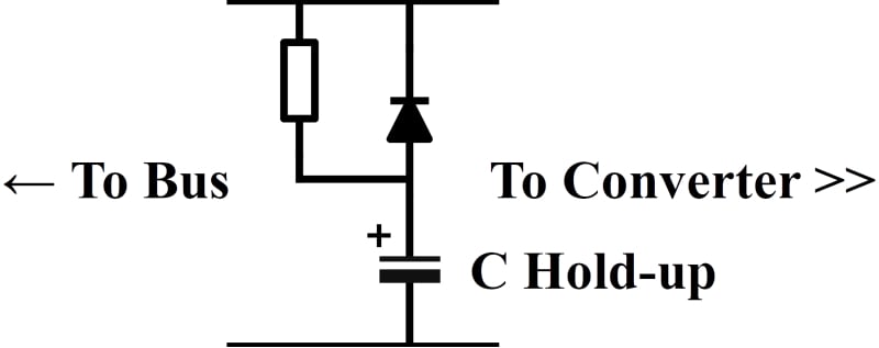
Figure 5. The simplest way to achieve the hold-up function requires a large capacitor and a power resistor bypassed by a power diode. Image used courtesy of Bodo’s Power Systems [PDF]
To address these challenges more efficiently, GAIA has developed a tiny hold-up module that boosts the 28 V bus voltage up to 80 V during normal operation. This solution significantly reduces the required capacitance by nearly a factor of 10 in our example, bringing it down to around 1580 µF.
\[C=\frac{2\times Power\times Time}{MaxVoltage^{2}-MinVoltage^{2}}=\frac{2\times100\times0.05}{28^{2}-9^{2}}=14220\mu F\]
Figure 6. The hold-up capacitor value remains large if it is charged only at 28 VDC.
Beyond energy storage, these hold-up modules offer a range of critical functions like adjustable power-fail detection to precisely match the converter’s minimum input voltage, adjustable capacitor voltage to optimize the energy storage, reverse polarity protection, and many more features. Over time, GAIA has built a range of holdup solutions, making life easier for designers while reducing the PCB space once occupied by bulky capacitor banks.
Table 1. Capacitance reductions were achieved for a 50 W power supply requiring a 100 ms hold-up time. This reduction is made possible thanks to the hold-up modules.
|
Configuration: |
With |
With |
With |
With |
With |
|
Needed capacitor value |
14224µF 50V |
7330μF/50V |
2450μF/80V |
1580μF/100V |
31330μF /25V |
|
Capacitor voltage |
28Vdc |
38Vdc |
65Vdc |
80Vdc |
20Vdc** |
|
Capacitor volume(in3)* |
3.34 |
1.5 |
1.2 |
1.16 |
2 |
* Based on a typical aluminium capacitor available
** These two models do not boost capacitor voltage but leverage the lowest volume that 25V aluminium capacitors offer
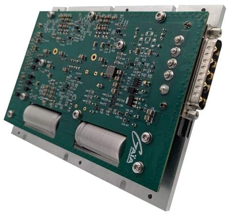
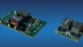
Figure 7. Only two small aluminum capacitors enable this DO-160-compliant 120W power supply architecture (GRD-12) to continue operating during a 50 ms input bus interruption. This is made possible by the internal holdup module. Image used courtesy of Bodo’s Power Systems [PDF]
Once the principles of conducted noise propagation are fully understood, effective filtering becomes a straightforward exercise. This is particularly true with GAIA’s integrated filters. Furthermore, meeting challenging bus interruption requirements like those in DO-160 or MIL-STD-704 is easily achieved using the company’s hold-up modules.
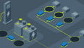
Their ability to reduce the hold-up capacity value for any interruption duration takes care of compliance without the need for large, board-space-consuming capacitors. The functional diagram in Figure 8 illustrates the concept of a compliant modular power supply architecture, in which each front-end component meets one or more specific requirements of the standards.
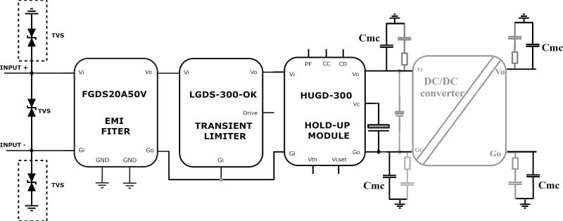
Figure 8. The front-end stage of a GAIA’s mil-aero compliant power architecture contains the TVS, the EMI filters, the transient limiter, and the hold-up module alongside the 2 hold-up capacitors. Image used courtesy of Bodo’s Power Systems [PDF]
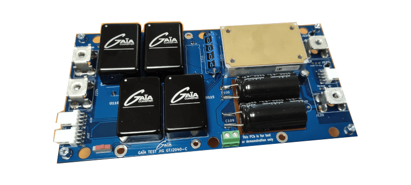
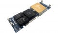
Figure 9. Example of a 250 W power architecture that can be built using evaluation boards, which are fully documented within the “evaluation board service manual” [3.2]. Image used courtesy of Bodo’s Power Systems [PDF]
As the front-end section of our compliant power architecture has now been defined, the 4th and last part of this article series will delve into the core of energy conversion. By leveraging the functions described, this part 4 will demonstrate how to construct a complete, standards-compliant power supply.
[3.1] https://www.vishay.com/docs/42115/ep2.pdf
[3.2] https://www.GAIA-converter.com/wp-content/uploads/application_notes/ EVGTJ2040.pdf
This article originally appeared in Bodo’s Power Systems [PDF] magazine.