Facebook
 Google
 GitHub
 Linkedin
New Ways to Produce Fast Power Thyristors
This article covers methods utilized at manufacturing of fast power thyristors by means of low-temperature junction of silicon chips with molybdenum discs.
Introduction
Traditional technologies of silicon wafer-thermal compensator junction do not comply with requirements for next-generation power semiconductors. Nowadays, low temperature baking (sintering) technology is spreading widely in semiconductor production. This technology is actual for junction of semiconductor chip with molybdenum discs for power and high power thyristors and diodes, designed for switching currents in the range from thousands to hundreds of thousands amps, and having the silicon chip diameter of 50 – 150 mm [1, 5].
Our experience with use of sintering at manufacturing of single-crystal power thyristors and diodes proves other advantages of this technology, including thermal cycling capacity improvement [3, 4], thermal resistance decrease [2, 3, 4], and surge current value increase [1]. Currently PROTON-ELECTROTEX masters manufacturing of power semiconductor devices by means of sintering. The article describes how characteristic of fast thyristors and diodes can be improved thanks to this technology.
Technological options of silicon chip-molybdenum disc junction
At present, there are two technologies utilized in the manufacturing of power thyristors: alloying and free floating silicon technology. Alloying technology joins silicon chip with molybdenum thermal compensator by use of vacuum soldering with aluminum-silicon alloys. This method provides firm silicon chip-molybdenum disc junction with good cycling capacity and quite low thermal resistance. External installation force from the cathode side is required to secure thermal contact.
However, since alloying is a high-temperature process (about 700C), thermomechanical stresses occur in Si-Mo packet because of different thermal expansion coefficients of silicon and molybdenum. This issue becomes even more significant for joined discs of bigger linear dimensions (diameters).
Another problem with alloying technology is active dissolving of surface layers of silicon chip. This issue is topical at manufacturing of fast-recovery devices as it is necessary to decrease the thickness of the silicon chip and generated anode emitter in order to secure the required performance characteristics. Thickness decrease and fusion penetrations lead to dispersion of emitter layer injection rate resulting in uneven spread of anode current.
Free-floating silicon technology puts a semiconductor wafer with cathode and anode metallization between cathode and anode thermal compensator of semiconductor device. Thanks to the absence of soldered joint, there are only pressure thermal and electrical contacts between molybdenum thermal compensator and silicon wafer. Pressure contact design’s advantage is absence of deformations and residual voltages that occur during soldering of silicon wafer with thermal compensator due to difference between linear expansion coefficients. This feature is extremely important for manufacturing of semiconductor elements with diameter of more than 80mm. Another important advantage of free floating silicon technology is that surface layers of silicon do not dissolve.
The disadvantage of this method compared to soldered contact technology is higher thermal resistance from the anode side.
Also, in order to avoid shorting of control area and cathode, mounting force is not to be applied to control area of thyristor. So this force does not spread on the same area from the anode side of the element.
As a result this may lead to issues with switching of high di/dt current pulse rise. This may also cause problems with low anode current operation of thyristors with auxiliary thyristor element securing control current of distributed control electrode (distributed gate) of main structure.
Non-soldering technology disadvantage described above is topical for power thyristors with semiconductor element of 80mm and more, as they need to have large and complex distribution area in order to provide required characteristics.
Growing demand for thyristors with higher power density and longer lifetime is a market trend, especially for high-frequency applications requiring fast thyristors.
That’s why the goal in manufacturing of fast power thyristors is to use the technology uniting advantages of soldered and free floating silicon approaches and narrowing down their disadvantages. This new technology needs to comply with following requirements:
- it needs to be applicable for large area elements;
- it needs to have low temperature of treatment process;
- it needs to have high electrical and thermal conductivities;
- its thermal cycling stability must be high.
Low temperature baking silver fine-dispersed layer technology (sintering) meets all these requirements.
On one hand, sintering technology provides firm junction with molybdenum disc and secures the element from partial dissolving of surface silicon layers. (Figure 1).
On the other hand, sintering technology decreases residual thermomechanical voltages and deformation profile on the semiconductor element. Experiments proved for sintered semiconductor elements to have 2 times lower bending of semiconductor elements compared to parts produced with soldering technology.
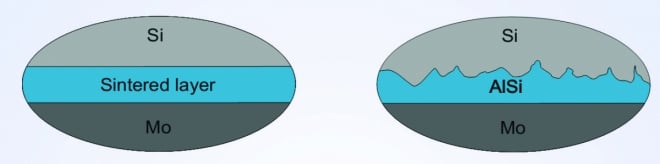
Figure 1: No partial dissolving of silicon surface layers on the anode side
Improvement of fast high voltage thyristors’ characteristics
Improvement of fast high voltage thyristors’ characteristics is shown by the example of TFI393-2500-28 thyristors (average current of 2500A, repetitive forward and reverse voltages of 2800V). These parts have 100mm semiconductor element diameter. They were manufactured of silicon wafers of 120Ω*cm resistivity and 580μm thickness. Two batches of TFI393-2500-28 thyristors were manufactured using different technologies of silicon chip-molybdenum thermal compensator joining.
Relations of main characteristics (on-state voltage drop VTM, turn-off time tq, reverse recovery charge Qrr,) are shown on figures 2 and 3.

Figure 2: VTM - Qrr relation of TFI393-2500-28 thyristors
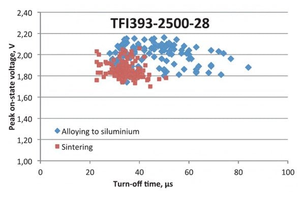
Figure 3: VTM - tq relation of TFI393-2500-28 thyristors
Figures 2 and 3 showing that thyristors produced with sintering technology have better VTM – tq, Qrr ratios. Absence of anode emitter melting positively affects the distribution of characteristics across the thyristor element area. Thus sintering technology helps making fast power thyristors with improved characteristics. (Figure 4).

Figure 4: Relation of TFI393-2500-28 thyristor’s main characteristics
Conclusion
Our experience with manufacturing of power single-crystal semiconductor devices using low-temperature sintering of silver paste proves that this technology can improve characteristics of fast diodes and thyristors. This technology decreases thermal resistance, turn-off time and reverse recovery charge of fast thyristors with 100mm semiconductor element diameter, decreasing on-state voltage drop and increasing root-mean-square current and on-state surge current in the same time.
About the Authors
Dmitry Titushkin works as a Research and Development Engineer at Proton-Electrotex JSC, a Russian company mainly involved in development, manufacturing and sales of bipolar power semiconductor devices — diodes and thyristors, power assemblies and IGBT modules.
Alexey Surma is head of Research and Development Center at Proton-Electrotex, a Russian company, which develops and manufactures power semiconductor diodes, thyristors, modules, heatsinks, IGBTs and power units for various electric energy converters. The company was founded and started production in 1996. As the head of R&D Center, Mr. Surma is mainly responsible for the development of new technologies and products.
Anatoly Chernikov is the Deputy Technical Director for New Technology at Proton-Electrotex, one of the leading Russian companies in terms of development and production of high-power semiconductor devices: diodes, thyristors, modules on their base, heat-sinks.
Sergey Matyukhin works as an Associate Professor at the State University — Education-Science-Production Complex (EPSC) where he also acts as a docent.
References
- H. Schwarzbauer. Novel Large Area Joining Technique for Improved Power Device Performance. - IEEE Transactions on Industrial Applications, 27 (1), 1991, p. 93- 95.
- A. Chernikov, A. Stavtsev, A. Surma. Features of wafer - Mo joining by sintering of silver paste for large area silicon devices. – Proc. EPE’2013, Lille, 2013
- U. Scheuermann, P.Wiedl. Low Temperature Joining TechnologyA High Reliability Alternative to Solder Contacts. - Workshop on Metal Ceramic Composites for Functional Application, Vienna, 1997, p 181-192.
- C. Göbl, P. Beckedahl, H. Braml. Low temperature sinter technology Die attachment for automotive power electronic applications. – Proc. Automotive Power Electronics, Paris ,2006.
- Dmitriy Titushkin, Alexander Pisarev, Alexey Suma. «Advantages of High Power Fast Thyristors and Diodes Produced by Means of Low Temperature Sintering of Silver Paste», in PCIM Europe 2015 Conference, 2015, pp. 899-905. Dmitri Titushkin, PROTON-ELECTROTEX, Russia, [email protected] , Alexey Surma, PROTON-ELECTROTEX, Russia, [email protected], Anatoly Chernikov, PROTON-ELECTROTEX, Russia, [email protected] Sergei Matyukhin, State Scientific Production University, Russia, [email protected]